Jun 09, 2015 · By Francoise von Trapp · 3D In-Depth
The GEMINI®FB XT fusion wafer bonding platform features up to a 3X improvement in wafer-to-wafer bond alignment accuracy as well as a 50% increase in throughput over the previous industry benchmark platform. These performance breakthroughs clear several key hurdles to the industry’s adoption of 3D-IC/TSV technology. Testimonial According to the...Jun 09, 2015 · By Francoise von Trapp · Blogs
The journey to the commercialization of 3D integration technologies has been long – longer than most expected – an arduous. It has required tremendous investment, and it has required the efforts of the entire supply chain. The industry has experienced a paradigm shift in how it conducts business because of...Jun 08, 2015 · By Herb Reiter · 3D Event Coverage
As promised in part 1 of my ECTC 2015 blog about this impressive conference, see below summaries of presentations I found very useful to contribute to the advancement of single- and multi-die packaging. To make it easier for the reader to dig deeper and review the entire paper, I included in...Jun 05, 2015 · By Herb Reiter · 3D In Context
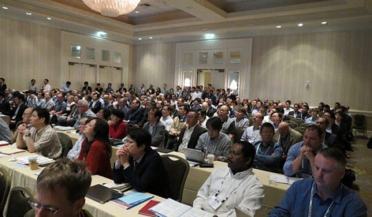
Last week I attended the record-breaking 65th ECTC in San Diego: 20 percent more attendees, compared to last year’s conference in Orlando. Once again, this year’s event offered a wide range of topics in six tracks. I spent most of my time in the “Advanced Packaging” track and was in...Jun 02, 2015 · By Francoise von Trapp · 3D Event Coverage
The Internet of Things (IoT) or as Cisco calls it, the Internet of Everything, has been the theme du jour for almost every semiconductor-related industry event in the past year, and going forward for 2015. The IoT hype continues, as many see the opportunity in this global trend to connect people,...Jun 01, 2015 · By Paul Werbaneth · Blogs
3D InCites / 3D+ recently had the opportunity to visit Dr. Robert Andosca, co-founder, president, and CEO of MicroGen Systems, Inc., at MicroGen’s headquarters in the High Tech Rochester Lennox Tech Enterprise Center, just off the Rochester Institute of Technology campus in Henrietta (Rochester), NY. To devotees of film, particularly...May 29, 2015 · By Francoise von Trapp · 3D Event Coverage
The 65th annual Electronics Technology Components Conference (ECTC 2015) logged record numbers (over 1500 attendees, 20% increase over last year) as the entire semiconductor industry recognizes (finally) that there is indeed money to be made in the advanced packaging sector. The flip chip and wafer level packaging sessions were full to...May 28, 2015 · By Paul Werbaneth · Blogs
The 26th annual SEMI Advanced Semiconductor Manufacturing Conference was held in Saratoga Springs, NY, May 3-6, 2015. ASMC 2015 drew a record number of attendees to the lovely old town of Saratoga (aka the Queen of Spas), a town which is conveniently situated just miles up the road from GLOBALFOUNDRIES Fab...May 25, 2015 · By Paul Werbaneth · Blogs
MEMS Industry Group®, the trade association advancing MEMS and sensors across global markets, announced the creation of its new TSensors division on May 14, 2015; headed by Dr. Janusz Bryzek, TSensors Summit, Inc.’s founder. MIG’s new division will extend TSensors Summit’s visionary efforts to accelerate a world in which everyone...May 20, 2015 · By Kevin Parmenter · Blogs
All the hype surrounding the Internet of Things has me worried. First of all, its my opinion that the motivation behind the IoT is not necessarily to our benefit. Call me a skeptic, but as I see it, like snake oil, we’re being sold on the notion that the IoT...May 15, 2015 · By Francoise von Trapp · 3D In-Depth
OmniVision’s OV23850 PureCel image sensor utilizes the companies advanced stacked die process capture exceptional images and video in 23.8-megapixel resolution while maintaining a compact form factor, which is critical for the next-generation of slim smartphones and tablets. Testimonial OmniVision’s family of PureCel backside-illuminated image sensors use the company’s stacked die...May 14, 2015 · By Paul Werbaneth · Blogs
The initial shock of a major earthquake lasts just a short time, tens of seconds, although it can seem forever for those trapped by its shaking. A tsunami wave train lasts minutes to hours before ocean waters re-stabilize after their initial disturbance. But the persistence of radiological disasters is measured...May 13, 2015 · By Francoise von Trapp · Blogs
Fan-out wafer level packaging’s star is clearly on the rise as a low-cost solution for consumer mobile products, and the semiconductor industry trade news has been buzzing with unsubstantiated claims that Qualcomm is ditching through silicon vias (TSVs) for monolithic 3D ICs (M3D) in its next generation of cell phones....May 11, 2015 · By Paul Werbaneth · Blogs
Join us in Milan, Italy, on September 17 and 18, 2015 for a new flagship MEMS event being produced by SEMI Europe. The SEMI European MEMS Summit 2015 expands on SEMI’s long record serving the MEMS device fabrication manufacturing supply chain and, combined with SEMI’s proven track record in microelectronics overall, the...May 06, 2015 · By Francoise von Trapp · Blogs
Today, LinkedIN reminded me that 3D InCites just celebrated its 6th anniversary. I also noticed that Paul Werbaneth’s latest 3D+ post, Japan, Abenomics, IoT, and the MEMS Engineer Forum 2015, was the 1001st post to be published on the site. That’s a lot of talk about 3D integration, from processes...Apr 30, 2015 · By Paul Werbaneth · Blogs
MEMS sensors, and the Internet of Things data they feed to the cloud, are being called on to jumpstart the world’s third largest economy. The economic revitalization strategy being instituted by Japanese Prime Minister Shinzo Abe, and now being carried out in Japan under the moniker “Abenomics,” consists of Three...Apr 29, 2015 · By Francoise von Trapp · 3D Event Coverage
ECTC 2015 returns to my favorite of its three rotating locations at the Sheraton San Diego Hotel and Marina almost exactly one month from now, May 26-29, 2015. This year, the ECTC technical committee has selected 350 papers on topics related to 3D and TSV technologies, wafer level packaging, electrical and...Apr 28, 2015 · By Herb Reiter · 3D Event Coverage
On Thursday and Friday of last week, Monterey, California’s previous state capital, became the center of presentations and discussions about IC design challenges as well as latest innovations / progress made in the field of EDA tools and IC design methodologies at Electronic Design Process Symposium (EDPS) 2015. We also learned a...Apr 27, 2015 · By Amy P. Lujan · Resource Library
Last year, I did an analysis that included the topic of wafer-to-wafer bonding. Specifically, it was a comparison of the three variations available when stacking wafers and/or die—wafer-to-wafer (W2W), die-to-wafer (D2W), and die-to-die (D2D). The goal of that project was to build cost models for W2W and D2W (with the...Apr 22, 2015 · By Francoise von Trapp · 3D Event Coverage
At the recent Arizona SEMI Breakfast Forum, held April 17, 2015, semiconductor suppliers gathered at the Mother Ship (aka Intel) in Ocotillo, AZ, to hear information that could affect their sales of tools and materials, based on the expectations of industry capacity expansion over the coming years. As the theme for the...