


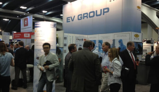
The 2015 3D InCites Guide to 3D at SEMICON West
2015 will go down in history as the year 3D finally got real. It’s not an emerging technology anymore, and as such isn’t a main feature at the 2015 SEMICON West, which gets underway next week, July 13-16, 2015 at the Moscone Center in San Francisco. Rather, this year 3D...
Lam Research: SABRE 3D
SABRE® 3D is a next-generation electroplating product designed to meet leading-edge production requirements for advanced packaging applications. This product leverages proprietary front-end manufacturing technology and offers market-specific solutions for copper pillar and through-silicon via (TSV) fabrication. SABRE 3D offers industry-leading throughput along with reduced cost of consumables to enable high economic value...
Nordson ASYMTEK: Programmable Tilt + Rotate 5-Axis Fluid Dispenser
Nordson ASYMTEK’s programmable Tilt + Rotate 5-Axis Fluid Dispenser dispenses using 5 axes instead of 3. The X and Y tilt enables dispensing from a vertical position, varying tilt angles to all sides of a component and up to the top of a 3D stacked die with high precision and...
Mentor Graphics: Xpedition Package Integrator
Xpedition® Package Integrator provides a holistic co-design methodology that automates planning and optimization of connectivity from a chip through multiple packaging variables, while targeting multiple PCB platforms. Engineers can quickly and easily assemble complete cross-domain systems (IC, package & board) and drive ball map plans and pin optimization through a...

Will the Internet of Everything Really Make the World a Better Place?
I recently started watching the HBO sitcom, Silicon Valley. If you haven’t seen it, it’s a great parody of what life in the Valley taken over by socially awkward technology geniuses looks like. It’s pretty funny, and a little bit scary. In one episode, the Pied Piper team is presenting...
Dow Corning: Thermally Conductive Gel TC-3040
TC-3040 is designed for advanced flip chip devices requiring improved heat dissipation. The material features a combination of low modulus and high elongation – enabling it to accommodate warpage-induced stresses. Key to the improved thermal performance : low contact resistance that silicones are known for, along with proprietary filler technology. Testimonial While...
SPTS: Sigma fxP PVD with Multi-Wafer Degas
SPTS’s Sigma® fxP, is a well established PVD system used in advanced packaging applications such as UBM and RDL. It utilizes batch degas technology that can improve Rc whilst maintaining high throughputs, despite the outgassing challenges posed from the increasing use of organics, such as mold in Fan-Out WLP. Testimonial...
Broadpak: 2.5D/3D Package Security IP
Industry’s first 2.5D/3D security IP from BroadPak provides trusted security and resilience needed for critical 2.5D/3D system integration and prevents hijacking of critical data. This new technology is shifting the paradigm in semiconductor industry and enables chip makers and system companies to develop new generations of secure products. This breakthrough...
Dow Electronic Materials: SOLDERON™ BP TS 6000 Tin-Silver Chemistry
SOLDERON™ BP TS 6000 Tin-Silver is a lead-free chemistry for solder bump applications. From a single formulation, it is capable of plating speeds of 2-9+ µm/min, tunable composition and the industry’s most robust process window. This flexibility makes it ideal for applications from C4 bumping to micro-Cu pillar capping. Testimonial...
KLA-Tencor: CIRCL-AP™
CIRCL-AP™ is a cluster tool with multiple modules, covering all-surface inspection, metrology and review at high throughput for efficient advanced wafer level packaging (AWLP) process control. The CIRCL-AP provides production-proven, high sensitivity monitoring capability for multiple AWLP applications including 2.5D/3D integration, wafer-level chip scale packaging and fan-out wafer-level packaging. Testimonial...

Path Finding and 3DPF
In the past year, I have written short pieces explaining how Path Finding methodology can proactively help identify viable solutions or reactively identify solutions if something changes during manufacturing. The next few blogs will look at specific examples using a PF tool to help separate the ‘wheat from the chaff’....
Indium Corporation: Wafer Flux WS-3543
Indium Corporation’s wafer bumping flux WS-3543 is a low-viscosity semiconductor-grade flux, specifically optimized for uniform solder bump formation across wafers up to 300mm (12 inches) in diameter. WS-3543 washes off completely, even after repeated application, reflow, and cleaning cycles, as may be seen in bump rework and after probe testing....

DAC 2015 Focuses on the Automotive Market
By attracting 7011 EDA and IP developers and users, the 52 Design Automation Conference, held in the South Hall of San Francisco’s Moscone Center in the week of June 7, achieved a 14.5% increase in attendees. I was one of them, and started on Sunday evening by listening to Gary Smith’ EDA...
Amkor: SLIM
Amkor’s SLIM (siliconless integrated module) is a dies-last package technology providing the thinnest possible form factor with the highest level of integration by use of back-end-of-line technology combined with assembly-based fan-out architectures. It has optimal registration, 3D access to top and bottom side of package and the finest line RDL capability...

Amkor Execs Outline Strategy for the Future of Advanced Packaging
I was invited to attend Amkor’s bi-annual customer symposium, which was held in Santa Clara two weeks ago. It was a grand event, complete with rock music intros narrated by a disembodied Voice of Authority for the execs (wait, was that AC/DC’s Back in Black I heard as CEO Steve...

Xilinx: Ultrascale VU440 3D FPGA
The Xilinx Ultrascale VU440 3D FPGA is constructed using “Xinterposer” 3D IC technology jointly developed by Xilinx and TSMC. It uses a low-k dielectric chip fabricated on 20nm silicon node with a total of 375,000 micron bumps stacked on 25mm x 45mm silicon interposer and assembled with CoWoS. The composite 3D FPGA consists...
Executive Viewpoint: The Impact of Process Control on FOWLP and 3D IC
As Si interposer and 3D stacked memory devices enter into production, albeit in low volumes, semiconductor manufacturers are lining up their ducks to be ready for high volume manufacturing (HVM) when it happens. As a result, some suppliers of high volume manufacturing equipment who have been rather quiet through the...
Dynaloy: Dynastrip DL9150
The newly released Dynastrip™ DL9150 is a non-TMAH containing multi-purpose photoresist and post-etch residue remover. With outstanding cleaning and metal compatibility, this product raises the bar for achieving environmental, health, and safety compliance while also performing as well as comparable products that contain TMAH. Testimonial: Dynaloy’s new solvent, Dynastrip DL9150,...

Sensors Expo 2015 and The Internet Of Messy Things
What are the implications for the Internet of Things when the “Things” are human beings? As was said in a recent New Yorker piece on exploring Mars, “… humans are the wrong stuff. They shouldn’t even be trying to get to another planet. Not only are they fragile, demanding, and...

Diverse Technology Selections Served at CS MANTECH 2015
What were all these silicon people doing at a compound semiconductor conference? CS MANTECH 2015 was the 30th anniversary version of the conference once known as GaAs MANTECH, and which now goes by the more representative name of Compound Semiconductor Manufacturing Technology Conference, the change made along the way to...