Jan 31, 2016 · By Francoise von Trapp · Blogs
During the 2015 European 3D TSV Summit, I drove attendees to distraction by asking each presenter what success looked like to them for 3D integration. The resulting responses became a blog post, What Does Success for 3D Integration Look Like? Now, a year later, I decided to revisit the topic by...Jan 31, 2016 · By Francoise von Trapp · Blogs
Now that we’ve determined that advanced wafer level packaging — including embedded technologies, fan-out wafer level packaging, and 3D packaging — add value to the devices in which they are implemented, the next step is understanding which option offers the best cost/performance ratio for specific product applications. One of the...Jan 28, 2016 · By Francoise von Trapp · Blogs
Hands-down, the best part of last week’s 2016 European 3D Summit was the Gala Dinner at the Chateau Sassenage, and in particular, the Gala Quiz. (I think my co-attendees would agree with me.) I applaud the organizing committee, and in particular Anne-Marie Dutron and Yann Guillou, for coming up with...Jan 26, 2016 · By Francoise von Trapp · Blogs
As it has in year’s past, the 2016 European 3D Summit kicked off with a market briefing. We heard from the usual suspects: Yole Dévéloppement (Rozalia Beica) and TechSearch International Inc. (Linda Bal). Additionally, in a nod to the business-centric tone of the conference, the committee invited Christian Knochenhauer, McKinsey...Jan 25, 2016 · By Francoise von Trapp · 3D Event Coverage
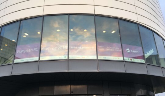
In its fourth edition and with a new name, the European 3D Summit (formerly the European 3D TSV Summit) reflected the shift from R&D to the real business of 3D integration and advanced packaging, and highlighted the significant growth this market space has undergone in the past year. It has...Jan 22, 2016 · By David Butler · Blogs
In contrast to some of the gloomier predictions of the analysts, we think 2016 will be a growth year for our business. In packaging, we see a number of development projects moving into production this year, and a raft of makers adding capability to catch up with the early adopters....Jan 22, 2016 · By Peter Ramm · Resource Library
Fraunhofer has been working on 3D integration for the past three decades, starting in1987 with a consortium of Siemens, AEG, Philips and the Munich institute IFT (now EMFT). By 1988, we could successfully fabricate 3D CMOS devices based on recrystallization of deposited poly-Si. In the mid-1990s, we developed a complete process flow...Jan 18, 2016 · By Haris Osman · Blogs
Heterogeneous integration is in many ways different from other research technology platforms. For one thing, the technology is mostly driven by specific customer needs and hence extremely difficult to anticipate. For some applications, we need to build, on top of CMOS, various sensors, filters, fluidic channels or photonics circuits. For...Jan 14, 2016 · By Garry Pycroft · Blogs
According to TechSearch International, we can expect to see 87% CAGR for fan-out wafer-level packages (FOWLP) over the coming 3 years. This demand is driven by a combination of several factors. Primarily there is great potential for the advanced capabilities of FOWLP to provide cost-effective system-level solutions for mid- to...Jan 12, 2016 · By Andrew Walker · Blogs
“On average since 1885, the yearly height record has gone up by 10 feet (3 meters) each time. Since the 1960s the pace has picked up to 16 feet.” This is not 3D NAND Flash but skyscraper heights in a recent article in The Economist (the power of visual data presentation!)....Jan 11, 2016 · By Bruno Morel · Blogs
2015 was a year marked by through silicon via (TSV) productization for three memory applications and a push for more MEMS and sensor technologies, as connectivity goes beyond computer-to-computer to thing-to-thing. For aveni, 2015 brought a new name, and leaps forward in commercializing our wet, molecular buildup process that provides...Jan 07, 2016 · By Bill Martin · Blogs
If I had not attended the 2015 3D ASIP conference, my outlook for 2016 would have been less upbeat for complex packaging (2.5/3D). But this conference showed that companies and their development organizations are NOT solely looking towards FinFETS and sub 20nm silicon process nodes to meet their integration, power,...Jan 06, 2016 · By Paul Werbaneth · Blogs
You can’t have the perpetual motion machine I received for Christmas this year, at least until I patent it. And the candy’s mostly gone. But there is something I would like to share with you, readers, and that something is beginning-of-the-year thoughts about connected things. It is a heavy responsibility...Jan 05, 2016 · By Francoise von Trapp · Blogs
In many of its implementations, the Internet of Things (IoT) certainly promises to improve our lives. But there are concerns about the potential trade-off: security breaches and relinquishment of privacy. While many are just realizing the implications, it’s been on the mind of Geoff Mulligan, executive director, IPSO Alliance, for quite...Jan 04, 2016 · By Eric Beyne · Blogs
For the past 2 to 3 years, 3D integration technology has developed into a technically and economically interesting road for further improving the performance of systems. In comparison to conventional planar 2D systems, we are now able to fabricate shorter and faster connections between circuits. And we can make these connections...Jan 01, 2016 · By Francoise von Trapp · Blogs
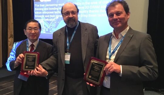
For the first time since the 3D Architectures for Semiconductor Integration and Packaging (3DASIP) Conference was established, the organizing committee decided to acknowledge the work of two researchers who were instrumental in developing the core processes that enabled 3D TSV development. In a brief ceremony, Dr. Phil Garrou presented 3DIC Pioneer...Dec 29, 2015 · By Herb Reiter · 3D In Context
While the shopping malls and specialty stores in and around San Francisco were packed with people hunting for Holiday presents, a very dedicated crowd of 3D IC developers and users from all over the world got together near San Francisco, for the 12th 3D ASIP conference, which featured, once again,...Dec 20, 2015 · By Francoise von Trapp · 3D Event Coverage
Staying relevant in the ever-expanding technology landscape that is the semiconductor packaging industry can be a struggle for an event that’s been laser-focused on one emerging segment since its inception. But this past week, 3D Architectures for Semiconductor Integration and Packaging (3D ASIP 2015) delivered a program that not only addressed...Dec 18, 2015 · By Francoise von Trapp · Blogs
Happy Holidays!Dec 15, 2015 · By Sundar Narayanan · Resource Library
The Opportunities for RRAM Cells to Take 3D Stackable Memory to 8-nm Nodes In Part One of this two-part series, we looked at the challenges that need to be overcome in manufacturing 3D stackable memory using the competing technology approaches. We will now focus on the advantages inherent in resistive memory...