Apr 06, 2016 · By Paul Werbaneth · From Different Dimensions
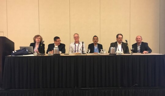
Keizai Silicon Valley, the organization here promoting network-building as a means of achieving successful US-Japan business relations, put on one of the most interesting programs this past week that I’ve attended year-to-date; a Keizai Silicon Valley panel discussion focused on “Trends in AgTech: Real Needs in the Industry.” Without looking, how far do...Apr 04, 2016 · By Martin Keim · Blogs
Solutions for 3D IC test are ready today, but they will be more ready tomorrow. At the 2015 ISTFA, I presented a tutorial titled “What is New in 3D, Digital Testing?” and I’ll summarize the main points here. I consider test standards and test challenges, which include known-good-die and testing...Apr 01, 2016 · By Francoise von Trapp · 3D In-Depth
For the first time ever, the Materials Research Society (MRS) brought its annual Spring meeting to Phoenix. I have never attended this event, as it is deeply academic, and has not been on my radar for 3D or advanced packaging technologies. However, after finding out from fellow SemiSisters, Rozalia Beica,...Mar 30, 2016 · By Ehrenfried Zschech · Resource Library
Advanced packaging, and particularly 3D through silicon via (TSV) integration technologies and the resulting 3D-stacked products, challenge materials and process characterization. For 3D TSV stacking of wafers or dies, die-to-die interconnections like micro solder bumps (e.g. AgSn) and Cu pillars are used. The control of the TSV filling and micro-bump...Mar 25, 2016 · By Amy P. Lujan · Resource Library
Through silicon via (TSV) technology is a key design element being incorporated into more and more advanced packaging designs today. TSVs offer distinct benefits in form factor and improved performance and can enable new, innovative designs not previously possible. To scale this valuable technology and spark industry adoption, there is...Mar 22, 2016 · By Francoise von Trapp · Blogs
This year’s keynote talks at the 2016 IMAPS Device Packaging Conference (DPC 2016) provided some new insight into a number of interesting areas of importance to the advanced packaging community. I already addressed Bill Chen’s talk, which focused on system-in-package (SiP) and introduced a 3D Fan-out SiP approach. Here, I’ll...Mar 20, 2016 · By Francoise von Trapp · Blogs
“The sum is greater than the whole of its parts.” ~ Aristotle (and Bill Chen) While the technology tracks offered the latest developments in interposer and 3D IC processes, fan-out, wafer-level packaging, flip chip, MEMs, sensors and more, System-in-package (SiP) was the big story of the 2016 MAPS Device Packaging...Mar 19, 2016 · By Herb Reiter · 3D In Context
Earlier this week I had the opportunity to attend this year’s TSMC Symposium. Just like in many previous years, TSMC had a lot of progress to report and demonstrated that they have a clear vision of the road ahead. As I expressed in previous years’ blogs, I started to get...Mar 19, 2016 · By Paul Werbaneth · Blogs
Collected impressions of 2016 to date: the unfortunate passing of too, too many favorite musicians; the hard-to-escape-from strident bellicosity of our national political campaigns; a winter of welcome, abundant, Northern California rains; along with a plethora of riches in the Silicon Valley conference, symposium, and seminar vein. Take the January...Mar 11, 2016 · By Herb Reiter · 3D In Context
The Computer History Museum in Mountain View is a very impressive place to show you the enormous progress ICs and Electronic Systems have made in the most recent 50+ years. What I like even more is the fact that an increasing number of high-tech companies and industry organizations are utilizing...Mar 11, 2016 · By Francoise von Trapp · Blogs
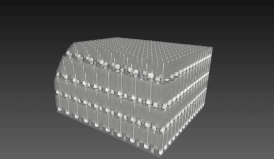
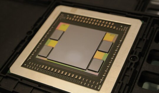
Last June, AMD made 3D integration history with its introduction of the Fiji gaming processor unit (GPU), which for the first time put high bandwidth memory (HBM) — a true 3D stack integrating memory die with through silicon via (TSVs) — into production. Fiji is a Si interposer-based module comprising...Mar 09, 2016 · By TechSearch International, Inc. · 3D In-Depth
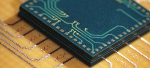
With the proliferation of mobile electronic products and the ongoing push for greater functionality in a smaller area, miniaturization has become a key word for system-in-package (SiP). SiP provides increased functionality in a subsystem that can be more cost-effectively assembled into a system. Miniaturization and other technology trends driving SiP...Feb 23, 2016 · By Francoise von Trapp · Blogs
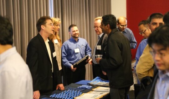
It’s been two years since I last visited EV Group headquarters in Schärding, Austria, so I was glad to be able attend EVG Technology Day on February 17, 2016 at the Fremont Marriott, in Fremont CA. It was a good reminder of the company’s many and varied capabilities in processes targeting 3D...Feb 19, 2016 · By Riko Radojcic · Blogs
Much has been written about the challenges that corporations face – especially established corporations – in adapting to a disruptive technology and the associated paradigm shifts. Most of the tomes on the subject focus on corporate management strategies. My intent is to discuss these challenges from a technology point of view...Feb 18, 2016 · By Robert Kavanagh · Blogs
2015 overall was a mixed year for the materials sector in the electronics market, with a general slowdown in PC-related segments offset by continued growth in mobile smart phones and other handheld devices despite industry growth flattening out late in 2015. In 2016, market forecasts indicate some improved growth and...Feb 12, 2016 · By Francoise von Trapp · Blogs
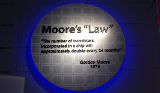
Now that the industry has finally called it a day for Moore’s law, will More than Moore be our guiding star for innovation? Analysts have been predicting the demise of Moore’s law for about as long as I have been covering 3D integration technologies. During that time, Intel has steadfastly...Feb 09, 2016 · By Jean-Christophe ELOY · Blogs
Over the past few years, it becomes clear that some panel-level packaging choices will be more suitable than others for successful commercial development. So, when will the panel-level packaging industry take off? How will it evolve? “At Yole, we’ve identified five key packaging platforms that can be processed on a...Feb 02, 2016 · By Herb Reiter · 3D In Context
DesignCon 2016 at the Santa Clara Convention Center gave football fans among us an opportunity to watch the preparation work for Super Bowl 50. Right across the street from the Convention Center is Levi Stadium, where on Sunday, February 7, this year’s champion will be crowned. Impressive, but let’s not...Jan 31, 2016 · By Francoise von Trapp · Blogs
During the 2015 European 3D TSV Summit, I drove attendees to distraction by asking each presenter what success looked like to them for 3D integration. The resulting responses became a blog post, What Does Success for 3D Integration Look Like? Now, a year later, I decided to revisit the topic by...Jan 31, 2016 · By Francoise von Trapp · Blogs
Now that we’ve determined that advanced wafer level packaging — including embedded technologies, fan-out wafer level packaging, and 3D packaging — add value to the devices in which they are implemented, the next step is understanding which option offers the best cost/performance ratio for specific product applications. One of the...