


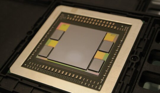
3D/TSV Officially Recognized as Advanced Manufacturing Technology at SEMI ASMC 2016
As Dick James, Chipworks, puts it, the SEMI Advanced Manufacturing Conference is “… an annual conference focused on the manufacturing of semiconductor devices; in this it differs from other conferences, since the emphasis is on what goes on in the wafer fab, not the R&D labs, and the papers are...

What is Driving the Advanced Packaging Market in China?
Driven by a strong semiconductor market outlook and aggressive investment in advanced packaging capability fueled by strong government support, advanced packaging revenue in China is expected to reach US$ 4.6 billion in 2020, against US$ 2.2 billion in 2015, announces Yole Développement (Yole). This market is showing an impressive 16%...
Supplier Updates from ECTC 2016
In addition to attending the panel and plenary sessions at ECTC 2016, which took place May 31-June 3, 2016, I also spent a good deal of time talking to industry suppliers to get updates on their latest accomplishments that will impact the future of advanced semiconductor packaging, including interposer integration...

DAC 2016: There is More to Life than IC Design
In the past, the Design Automation Conference was known to me and many of my colleagues as the annual event that focused on IC design tools, flows, and methodologies. EDA tools vendors and users got together in the previous millennium to discuss what to do next in a rapidly growing market...

Make Every Market Smarter: An Interview with SEMI’s Yann Guillou on the European MEMS Summit
SEMI’s first edition of the European MEMS Summit, which took place in 2015 in Milan, was a stellar success, attracting 265 attendees from 21 countries. The second edition will take September 15-16, 2016 in Stuttgart Germany; a fitting location as many MEMS producers are headquartered nearby. 3D InCites caught up...
ECTC 2016: Is the Life after Moore’s Law?
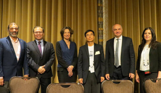
Is Moore’s Law dead or not? It depends on your perspective. Last week at ECTC 2016, Rozalia Beica, Dow Electronic Materials, gathered a prestigious group of senior executives from the world’s leading microelectronics research institutes to discuss Life after Moore’s Law. Panelists included Marie-Noelle Semeria, CEA-Leti; Dim Lee Kwong, IME;...
Words of Advice From Successful Women in Advanced Packaging
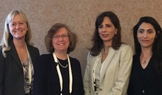
For the second consecutive year, Beth Keser, Qualcomm, organized and moderated the CMPT Woman’s Panel and Reception as part of ECTC’s special sessions. This year’s topic was titled, Maximize your Career Potential. Panelists included Jan Vardaman, founder, and president of TechSearch International, Inc; Rebeca Jimenez, SVP, Amkor Technology, Inc.; and...
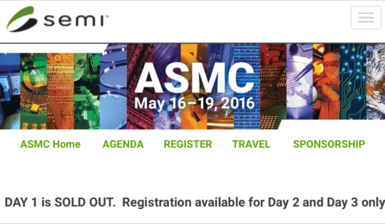
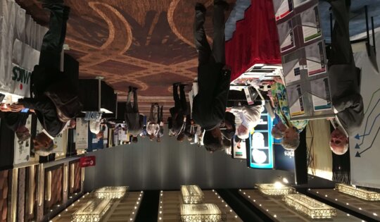
Moore’s Law Passes the Silicon Stress Test at SEMI ASMC 2016
Stress Test, noun: “A test designed to assess how well a system functions when subjected to greater than normal amounts of stress or pressure.” [Source: Oxford Dictionaries.] The 27th annual SEMI Advanced Semiconductor Manufacturing Conference was off to the races the week of 16 May 2016 in charming Saratoga Springs,...
ECTC 2016: Memory Technology Advances and Prospects for Packaging
At ECTC 2016, which took place at the Cosmopolitan Las Vegas, Las Vegas, May 31-June 1, 2016, the special session entitled, Memory Technology Advances and Prospects for Packaging may have been one of the “most important starts to ECTC ever.” At least that was TechSearch’s, Jan Vardaman’s impression, and I can’t disagree,...
Convergence on the “Big Five”: Focus on MEMS Packaging
Part three of a five-part series In the first two parts of this series, we focused on low-cost flip chip and wafer-level chip scale packages (WLCSP), identifying them as two advanced packaging platforms we consider to be among the “Big Five.” It is our belief at Amkor that convergence into...

Looking Beyond the Components Horizon at ASME’s IoT Connect.
Every time someone asks me how my years experience I have, I tend to get evasive or try to turn it into something funny. At a recent conference, the speaker before me admitted that he is OLD and told us that he has 30 years of experience in semiconductors. When it was my...

“How Do You Create The Future?” Through Innovations in Heterogeneous Integration and SiP
MEPTEC Luncheons returned big to The Bay Area on Wednesday, May 25, 2016, with a new venue (SEMI HQ), a new joining of forces (IMAPS-MEPTEC-SEMI), a great turn-out (fully committed, capacity-wise, as they say in the restaurant biz), and an inspiring talk by Bill Chen, ASE Fellow and Senior Technical...

Meet Me at ECTC 2016 in Las Vegas
With the industry-wide shift in focus from furthering Moore’s Law to the realization that 3D integration and advanced packaging technologies are the shining stars of the next generation of electronics, the 66th Annual IEEE Electronic Components Technology Conference, which takes place May 31-June 3, 2016, at the Cosmopolitan of Las...
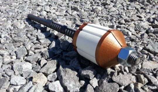
IPSO Challenge Update: The Smart Rock Bolt Success Story
Six months ago, I interviewed Jens Eliasson, associate professor at Luleå University of Technology (LTU), and co-developer of the Smart Rock Bolt, a vibration-sensor-based device used for instrumenting tunnels in mines to detect potential catastrophic collapses. He had just accepted the IPSO Challenge grand prize on behalf of his team. That...

Convergence on the “Big Five”: Focus on WLCSP
Part two of a five-part series. How did we determine which technologies are “the Big Five,” for semiconductor packaging? Essentially, we identified the five key platforms that we believe will be leveraged across a multitude of applications and markets now and in the future. The selected platforms are low-cost flip chip,...

ASMC 2016, the Return of MEPTEC Luncheons, and Your May Calendar
The Saratoga Springs, NY, horse racing season starts in late July, following a racing tradition that dates to the 1860s. That’s a pretty long run indeed, and it’s one of the things, along with the healing spring waters, successful Revolutionary War battle history, and “summering” by well-to-do Boston and New...

Challenges and Solutions for EDA of 3D Chip Stacks
It is often claimed that 3D chip stacks offer the potential to meet current and future requirements of digital circuits, such as for performance, functionality, and power consumption. Specifically, both design paradigms “More Moore” and “More than Moore” will benefit from 3D chip stacking (and new technologies and materials). 3D...

Transforming Today’s Semiconductor Industry Challenges into Tomorrow’s Opportunities
My wife, born and raised in Hong Kong, tells me that the Chinese language uses the same word for challenge and opportunity. What can we, in the 200-year-old US of A, learn from the 4000 years old Chinese culture? The Chinese have a point! Based on my personal experience, I...

What to Expect on 3D Integration and IoT at the 2016 Symposium on VLSI Technology
If you’re planning to attend this year’s combined Symposium on VLSI Technology and Circuits, themed “Inflections for a Smart Society,” which takes place June 13-15, 2016 in Honolulu, HI, and you’re primarily interested in advancements in 3D integration and Internet of Things (IoT), here are some not-to-be-missed papers to put...
Convergence on the “Big Five”: Focus on Low-cost Flip Chip
Part one of a five-part series. Over the past few years, there has been a significant shift from PCs and notebooks to smartphones and tablets as drivers of advanced packaging innovation. In an industry segment that has grown accustomed to a multitude of package varieties, we believe we are now...