


Mentor Graphics: Calibre
Product Description Calibre enables signoff verification of chip stacks with flip chips, silicon interposers and through-silicon vias (TSVs). Verification of individual dies is followed by checks on the interfaces between dies, including dimensional checks (bump alignment and rotation), connectivity checks (LVS), and parasitic extraction (PEX) using a special 3D-IC rule...
ALLVIA: Silicon Interposers for Electro-Optical Engines
Product Description 2.5D Silicon Interposers form the base for the assembly of electro-optic engines for Chip-to-World Interconnects. These electro-optic engines with TSVs, the foundation for so-called “active cables”, offer outstanding Interconnect Bandwidth Density. They operate at 10 Gb/s today and are expected to migrate to 25 Gb/s or higher in...
E-System Design: Sphinx 3D Path Finder
Product Description 3DPF is a full wave 3D path finding tool based on a patented, mesh-less algorithm for cylindrical objects (vias and bond wires). By not meshing cylindrical objects, significant memory and CPU time is saved allowing users to analyze much larger structures in a much shorter time. Testimonial From Sherry...
3D IC Blogosphere Update – Feb 22
Has it really been a month since the European 3D TSV Summit? This inaugural event certainly caused a buzz in the blogosphere! In addition to all my coverage after having attended the event, Phil Garrou has been slogging his way thorough the proceedings to provide an in-depth review on Insights...
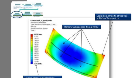
Tips on Modeling Warpage for 3D ICs
This week’s webinar on chip stack assembly simulation, presented by Kamal Karimanal of Cielution offered some useful information on how modeling can be used to minimize warpage in 3D stacking. In 3D stacking, versus traditional flip chip processes, thickness of RDL layers in comparison with the thinned die or wafer can lead...
Multi-Die Integration Provides Multifaceted Solutions
Multi-Die Integration Provides Multifaceted Solutions By Francoise von Trapp, 3D InCites This year’s Roadmaps for Multi-Die Integration Symposium, hosted by MEPTEC on November 14, 2012 at the Biltmore Hotel in Santa Clara, CA, offered some interesting and different perspectives than the garden-variety 2.5D and 3D IC conferences of late. While...
This Week in 3D IC News (Oct 8-12)
All Programmable PlanetToday All Programmable Planet’s newsletter appeared in my inbox, with a great post by Max Maxfield on the Xilinx family of 3D FPGAs. Beyond the detailed descriptions of Xilinx’ products, and explanation between the difference between 3D FPGA and 3D Heterogeneous FPGA, I especially like Max’s musings on...
Some 3D Technology Tidbits
Glass interposers got a thumbs up from i-MicroNews in a “Closer Look” post reviewing Corning’s Peter Bocko’s presentation at IMAPS 2012. Based on work done as part of Ga Tech’s consortium, Bocko demonstrated that “glass interposers show less warp during chip assembly, faster signal propagation and significantly reduced signal loss. In...
EDA Vendor Wins from TSMC
TSMC certainly did hand out keys to the city to the EDA vendors last week at OIP. Just to recap, we reported on Synopsys and Cadence CoWoS reference flow wins last week here and here. Mentor Graphics’ nod came in the form of Partner of the Year Award for “CoWoS...
3D IC Educational Opportunities
If you have an hour of professional development time coming to you, I advise that you spend it watching this webinar on TSV and Interposer: modeling, design and characterization, presented by Darryl Kostka, of Computer Simulation Technology (CST). But don’t just take my word for it! It comes highly recommended...
Important stuff – but first, some 3D Friday fun
Fridays just kind of creep up on you, don’t they? It’s been a busy week in the 3D blogosphere – and not just on 3D Incites. I’m a little disappointed that nobody wanted to play the “how do you use your mobile device” game I started on Monday with these...
SEMICON Taiwan’s 3D Tech Forum: Were You There?
I didn’t make it to the SEMICON Taiwan SiP Global Summit this year and was hoping to find some coverage by other journalists so that I could at least curate and share the information on the 3D IC Technology Forum. Unfortunately, I didn’t see anything posted on the topic, but...
The Stacked Die Reality Check Continues; FPGAs Lead the 3D Charge
It’s been one of those Mondays. I started making the coffee this morning (put in a clean filter, poured in the water) before I got sidetracked and hit the shower without ever putting in the grounds or turning it on. Then I left the Impress Labs office without my key...
Update on 3D transistors (That “other” 3D)
I always hesitate to cove 3D transistors, because before they came along, I only focused on what I knew to be 3D – ie: 3D stacked packages, 2.5D interposers and 3D ICs. And that was confusing enough. But then along came Intel’s Tri-Gate technology, claiming the 3D moniker as its...
SEMICON Europa 2012 Focuses on Materials, 3D ICs, and 450mm
SEMICON Europa got underway yesterday, and reports from the event point to new materials, 450mm and 3D ICs as the key topics – all from the European perspective. According to SEMI Europe President, Heinz Kundert, Europe has reached a critical crossroads where its very future as a global competitor seems...
When 3D is 3D IC, and When it’s Not
Some of the best news to read (especially on a Friday) is non-news, like this report by Ann Steffora Mutschler, in SemiMD on how 3D ICs will not impact computational lithography tools. According to her sources, this particularly true with regards to TSVs, because of their large size in comparison...
Today in 3D: HMCC Drafts Specs; Materials Suppliers take on TB/DB; OSATS add Capacity
I’ve come across a few interesting announcements in the 3D space today that separately are just random bits of news, but when bundled together, demonstrate acceleration to 3D commercialization. When you think about it, we’re more than halfway to Q1 2013, which has been earmarked by Micron as when 2...
Design and Test Solutions are Trending in 3D ICs
These days, as I troll the pages of the Internet in search of juicy tidbits of 3D IC news and information, I’ve realized that with the exception of that pesky issue with thin wafer handling, focus has moved away from novel manufacturing processes, and turned its magnifying glass onto the...
Invensas Unveils Groundbreaking Package-on-Package Solution for Next-Generation Smartphone and Tablet Computing
Invensas Corporation, provider of semiconductor technology solutions and wholly owned subsidiary of Tessera Technologies, Inc. unveiled its bond via array (BVA) technology. BVA is an ultra-high I/O packaging alternative to wide-I/O through silicon via (TSV) that delivers the performance required by mobile OEMs while preserving the proven infrastructure and business...
3D Company Updates
There are a couple of notable updates circulating this week involving companies in the 3D space. The first I saw was news from Sony that it has introduced its next-generation CMOS Image sensor they claim is “ the industry's smallest, CMOS image sensor and camera system”. The image sensor is...