
There are two key components to the ability to continue scaling integrated circuits (ICs): The ability to increase transistor density transistor and keep it functioning properly, and the ability of the interconnect to move the electrons from the transistor to the other ICs, or systems to which the logic chip is connected. The IEEE IITC conference has dealt with interconnect technology for over 20 years, documenting the transition from aluminum to copper, and now to cobalt and other metals that are being introduced to the interconnect stack.
The IITC does not just deal with the resistance of the metal. Techniques to reduce the capacitance of the dielectric still show up from time to time, but at the moment the dielectric or k values haven’t shifted much over the past few years. I used to be a regular attendee at the conference until they began to alternate locations between the United States and international locals, and the company I worked for, in its wisdom, decided I didn’t need to travel to view the event. So, this year with virtual attendance I was able to renew my attendance at the conference.
The technical sessions were kicked off by Mike Mayberry of Intel, speaking on “The Future of Compute: The Connected World meets the Interconnected Platform”, and H.S. Phillip Wong of TSMC and Stanford University. Speaking on “Technology for 3DICs” the two overviews covered at a high level most of what would be discussed over the next several days at the conference.
Mayberry explained that it’s all about the data and how new chip/system designs are needed to deal with distributed compute. Compute will be embedded throughout the cloud infrastructure all the way from the edge where the data is generated and first analyzed, to the cloud, which will be the source of for now a great deal of AI learning. To deal with disaggregation of the data you can use tiles to create the custom compute, thus combining, CPU, GPU, NPU, memory, and other technologies into a system. Combining all of these tiles together creates more interconnect, it also unfortunately at the moment uses more power. As a result, innovation is needed for scaling, new materials, nanoribbons, gate-all-around technology, and interconnect design. Bump pitch scaling and design of the wiring routing can help reduce the power consumption and perhaps improve system speed.
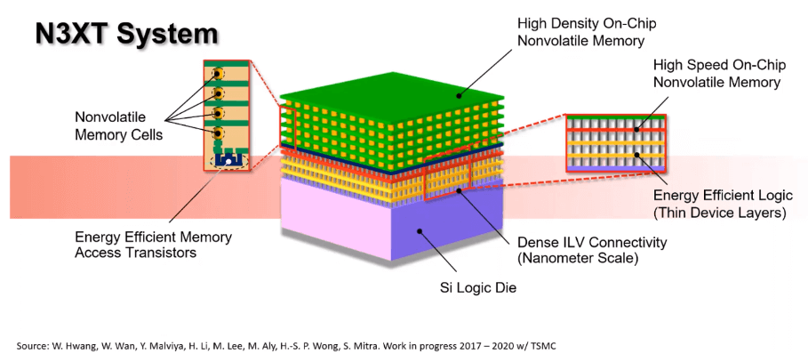
Dr. Wong reiterated much of Mayberry’s comments, with respect to AI driving the need for improved 3D compute for supercomputer applications. Wong discussed the need for optimizing the compute for the application. It is critical for memory to be readily accessible to the logic with adequate bandwidth. Currently, this is being done with high bandwidth memory stacks on the 2.5D or 3D package. Wong discussed TSMC’s N3XT 3D technology which layers the memory and the logic to enable higher processing speed. For more detail on the topic please see my co-blogger, Phil Garrou’s blog on the topic.
CEA-Leti and IMEC also presented on this at their co-seminar prior to IEDM last December.
(do you want to link my article to this)
Having been very involved in through-silicon via (TSV) development over the years, and the holy grail that is chip-to-chip packaging. I am still wondering how they will get the heat out; especially, with a greater density of transistors, and faster processing speeds. It is possible that new materials such as carbon nanotubes, which Wong touched on, will help to solve this problem, but carbon nanotubes have their own manufacturing issues and are a long way from production. Thus, only time and experiments will tell how tightly the industry will be able to package the logic, memory, and other devices in the near to distant future.
The Details of Interconnect Technology
From the 20,000 foot view, the conference very quickly gets down into the details of interconnect technology. Some of my highlights are below.
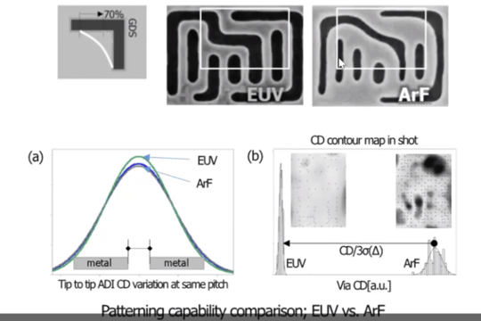
Multiple papers were presented on the sub-7nm interconnect technology. Samsung demonstrated the advantages of using EUV for a 7nm back-end-of-the-line process, while IMEC presented on the 3nm technology node. Consistent from the papers is that cobalt is replacing copper and the barrier liner at smaller pitches, and as scaling continues ruthenium will likely replace cobalt to keep the resistance at a manageable level.

IMEC proposed a new damascene technology called semi-damascene, which is needed to resolve the issues with interconnect scaling at the 2nm technology node. The process includes using Ru to replace Cu and airgap technology.
Selective tungsten seems to finally be successful, as it is deposited on metal and dielectric, not silicon.
Intel’s 10nm paper was a bit anticlimactic, given that an updated version of the technology was presented at architecture day.
Graphene, carbon nanotubes, and two-dimensional materials are making their way into the process flow’s at least in the R&D phase of the process.
IBM is still extremely active in the interconnect space.
Advanced Stacked ICs
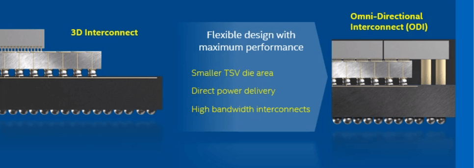
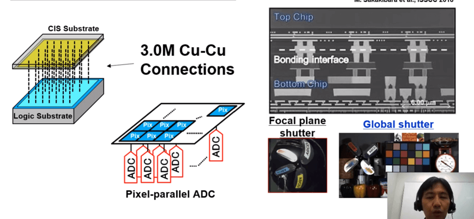
The key to smaller packages, and to a certain extent the success of 3D systems, is the shrinking of the bump pitch. Since the goal is to put different functional technology together in the same package in the smallest form factor possible, different bumping pitches are needed to accomplish this, in some cases much smaller than the industry is working with today. I was aware of work going on in the 10-25 µm range. At Intel’s Architecture Day, it was mentioned they are working on 10um pitches. So, when Sony presented at IITC on 1um pitch Cu-CU hybrid technology, I was a bit surprised. Sony demonstrated that they could successfully bond chips together with good electrical results. Sony showed that you could have up to 0.25um offset and still get good results. This work suggests that the ability to create smaller bump pitches than currently used is very possible in the near future.
The 3D InCites Virtual Event Scorecard
Having, like most of you, attended multiple video conferences over the past 9 months I’m developing my likes and dislikes of how organizations run these events. The voice quality was better than most, which is an improvement over many conferences. However, at the IEEE conference in June, I believe you were able to click through slides during the on-demand portion of the event. This was an excellent tool for when you wanted to go back and study the details on the slide. I also would have appreciated a bit more time to peruse the IITC conference information, I know they gave us 25 days but October was a busy virtual conference month.