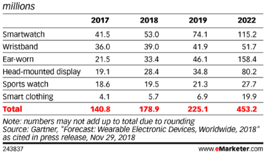
From November 5 to 7, 2019, I had the opportunity to attend the inaugural MEMS and sensors focused Microtech Innovation Summit at the DoubleTree Hotel in San Jose. I have to admit, until recently I didn’t follow MEMS and sensors (M&S) and didn’t notice the broad and rapid market acceptance of these products (Figure 1). They capture real-world data – which is analog and multi-physics – and feed data converters to translate it into zeros and ones for digital electronics. In addition to M&S and data converters, many Internet of Things (IoT) edge nodes are likely to also contain energy harvesters, processors, memory and I/O functions. Edge nodes are also likely to combine all these functions in one 2.5D-IC system-in-package (SiP) or module.
Also new to me were Microtech Ventures (MV) synergistic services, very useful for startups and larger companies. The organization offers strategy consulting, recruiting, business development, angel investments, venture capital as well as mergers and acquisitions advice. You may know MV already as the publisher of the MEMS Journal. This summit demonstrated clearly that MV can offer much more than this weekly newsletter.
In his introduction, Mike Penelis, President and CEO of MV, highlighted key questions this Innovation Summit wanted to address:
- What are the most promising areas of MEMS, sensors, and microtechnology innovation?
- Which technologies and applications to focus on?
- How to create value with M&S startups?
Then he discussed major market trends encouraging broad deployment of M&S:
- IoT is becoming a reality and M&S are essential ingredients
- Emergence and the increasing importance of AI/ML – they need useful data from sensors
- The increasing pace of M&S innovation and resurgence of “deep tech” startups
- Aging populations and “healthcare-focused” demographics
- Emergence and the increasing importance of advanced mobility, ADAS, and autonomous vehicles
Allow me to comment: Recognizing the above trends and responding to them vigorously is in stark contrast to the way semiconductor businesses were run in the past. Systems were built around chips — remember “Intel Inside” — as an important selling point for PCs and other electronic systems. These five trends clearly show that today’s system designs start with a specific application in mind. Trend #3 simply confirms that innovative executives are reacting swiftly to this paradigm shift, and developing a wide variety of functions to serve these applications.
The three-day Innovation Summit addressed many topics relevant to the M&S ecosystem and confirmed their important roles in Billions of IoT edge nodes:
- They give electronic systems up to 5 senses — to see, hear, smell, taste and touch their surroundings.
- Many edge nodes include intelligence to process data locally and initiate instant actions. In addition, such intelligent edge nodes consolidate data and transmit only summaries to the cloud. They reduce network traffic and data center loading, both contribute to minimizing power dissipation.
Short Course Summary
Day 1 was dominated by two in-depth short courses: Brian Zahnstecher from PowerRox discussed the importance of minimizing power consumption in the Billions of IoT edge nodes and outlined many ways of harvesting power, to minimize/avoid the costly and time-consuming battery-replacement routines.
Philip Feng, Professor at the University of Florida, gave a very comprehensive overview of how MEMS and NEMS (Nano ElectroMechanical Systems) contribute to Quantum Engineering. He also suggested reading “The Quantum Goldrush” article in a recent edition of NATURE magazine, to learn about the importance of Quantum Computing and how it impacts private investors.
Brief Summaries of the 40+ Presentations
To keep the length of this blog manageable, allow me to mention only key points for every session. For more info about speakers’ roles and affiliations as well as presentation titles, please go to the Summit’s website. If you want to know more about a topic, please search on the companies’ websites or contact Pinelis’ team. MV can provide you with information about every one of the companies mentioned in this blog and, if you are interested, they can add strategic value to your M&S specific activities and plan(s). MV’s website is here.
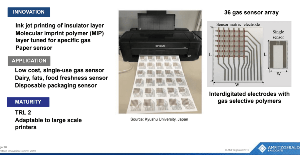
In addition to the short courses mentioned above, several start-ups described their relevant efforts. Alissa Fitzgerald, from AM Fitzgerald & Associates, outlined how to print sensors on paper or plastic to lower cost, helping to make sensors ubiquitous (Figure 2).
Other speakers described how a digital nose functions, how smaller feature sizes can increase sensors’ sensitivity, explained 3D microprinting and outlined the varieties of available gas sensors and their capabilities.
To summarize day two, let’s just say we drank information about M&S related innovations from a firehose from 8 am to 6 pm.
In the morning speakers from Applied Materials and General Electric talked about their M&S related work, outlined their companies’ Venture Capital activities and encouraged synergistic partners to open a dialog with them. Silterra, Teledyne Micralyne, Sony, imec, ULVAC and Suess also showed their commitments to M&S. In the afternoon UC Berkeley, Fraunhofer IPMS, Philips Innovation Services, and KST World described their diverse R&D efforts in support of M&S. In the following Technology Innovation Showcase, ten smaller companies talked about their contributions to expand the capabilities and value of M&S. In addition, the University of Pennsylvania talked about how they develop tiny robots and outlined potential applications for them.

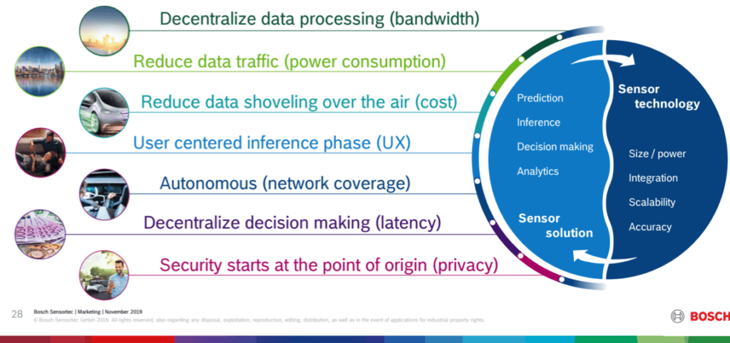
Day 3 started with a presentation by BOSCH Sensortech. Marcellino Gemelli described their broad product portfolio’s progression from only 1) reading data, 2) evaluating it, 3) learning from it. With the slide in Figure 4 below, he explained why more and more of a system’s functionality is moving to intelligent IoT edge nodes.
Next, Johnson & Johnson and TDK Ventures talked about their M&S activities and explained how they encourage and support start-ups. The SAES Group emphasized the important role materials play in assuring reliability and Fraunhofer IPMS presented their work on MEMS-based, low-power micro speakers.
During another Technology Innovation Showcase session the University Quebec, the FEMTO ST Institute, Harvard, and the founders of InchFab as well as Prophesee presented their R&D activities for micromachining of glass, robots for micro/nano manipulations, micropower supplies, low-cost 2” wafer for MEMS as well as bio-inspired vision.
Then InstruMEMS, Novasentis, Sigma Sense, and a graduate from UC Berkeley’s BSAC Institute presented solutions for real-time nanoscale sensing, haptic microactuators, capacitive imaging technologies and sockets for MEMS, respectively.
Microtech Ventures Innovation Summit Highlights from an EDA/Design perspective
Two presentations addressed this important topic. My thanks go to the conference organizers and these speakers:
- David Fried from OnScale explained how their cloud-based multi-physics simulator, in cooperation with accurate process design kits (PDKs), replaces expensive, lengthy and unreliable prototyping loops. See OnScale white paper here
- Equally important, Mary Ann Maher, SoftMEM’s CEO, talked about the expanding market for M&S, the need for MEMS Building Blocks (a.k.a. MEMS IP) to increase designers’ productivity and how her team develops MatLab, Verilog and/or Verilog A models, as solid foundation for above, jointly developed, MEMS design and verification flow. See more about SoftMEMS here.
- FYI, Mentor, a Siemens Business, OnScale, and SoftMEMS announced a week before this event that they’ll jointly develop user-friendly modeling, design and verification methodology for MEMS and sensors. A brief press release about these plans is here.
Exhibitors
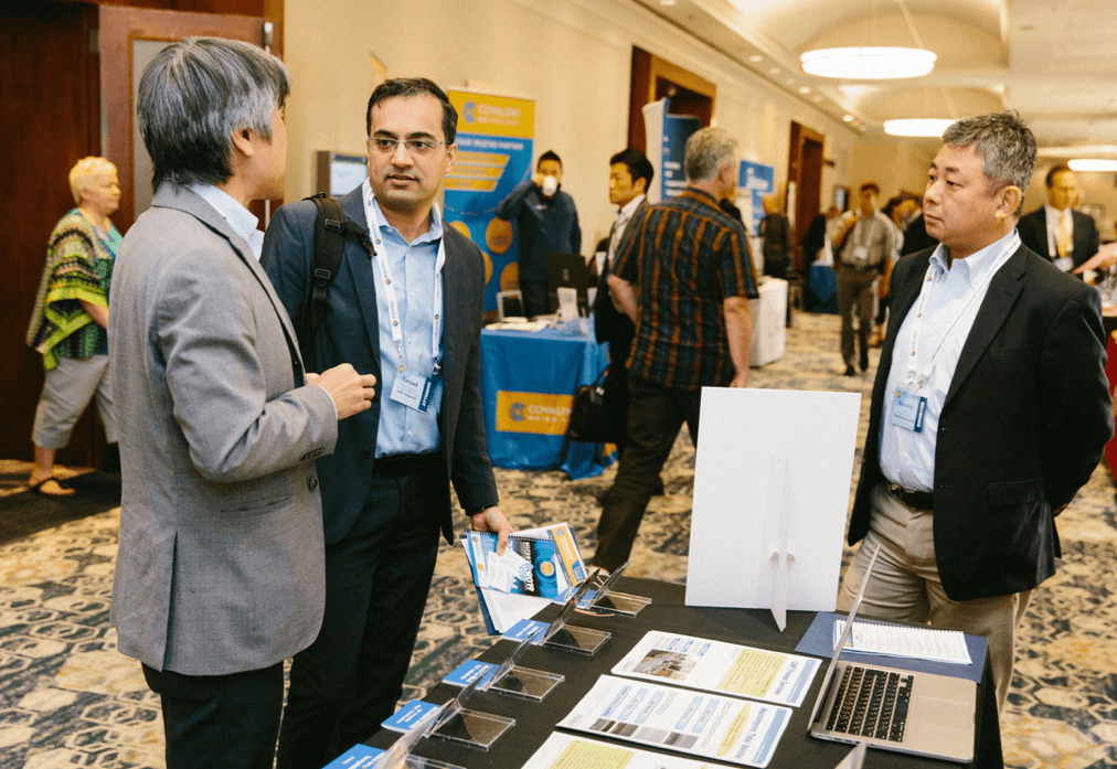
In addition to more than 40 companies and organizations presenting, about 25 exhibitors in the hallway engaged interested parties in in-depth discussions about market needs, current capabilities and plans.
Conclusion
This MEMS and Sensors Innovation Summit taught me several important points:
- The forecasted tens of Billions of IoT edge nodes will contain heterogeneous functions (logic, memory, data converters, RF, M&S,…) and must consume very little power – ideally, harvest the needed energy from the environment. Multi-die IC technology is well-positioned to meet all these requirements.
- Many innovative developers, at universities, start-ups, and large corporations, are committed to broaden M&S capabilities, improve accuracy, reliability, and ease-of-use, while reducing cost and form factor – to eventually give every system the five senses that make humans successful.
- AI/ML at the edge nodes and/or data centers will add a “sixth sense” to help to predict maintenance needs and improve the performance of human bodies and machines.
- To reap all these benefits, domain experts in many fields need to work together closely.
Events, like the recent Microtech Innovation Summit, as well as SEMI’s MEMS and Sensors Summit, which I attended in September, are excellent ways for building a well-functioning M&S ecosystem and bringing today’s 1,800+ sizeable/significant MEMS, sensors, and microtech companies closer together. Thanks for reading. ~ Herb
The Microtech Ventures 2020 Schedule
- ADAS Sensors 2020 in Detroit, Michigan, April 1 and 2, 2020
- Medical Wearables 2020 in San Jose, California, May 13 and 14, 2020a
- Automotive AI 2020 in Detroit, August 5 and 6, 2020
- Automotive Lidar 2020, in Detroit, September 22 and 23, 2020