Just in case you didn’t have a chance yet to read part 1 of the ISS 2019 blog, covering day 1, it’s posted here.
Technology and Manufacturing Trends
Day 2 started with a keynote about the magic nanodevices can create, delivered byJo de Boeck, imec’s EVP and chief strategy officer. He emphasized that we need to find smarter ways to compute, store data and connect building blocks. De Boeck expects that new device architectures, memory technologies, materials, and packaging/assembly techniques will contribute to the needed innovations. Like previous speakers, he stated that IoT edge devices do/will need significant compute and storage capabilities, possibly use neuromorphic techniques, and projected that one-third of the inference work will be done at the edge nodes. De Boeck praised the capabilities of 3D stacking as an important step towards making edge nodes more powerful and simplifying system-level integration in general (Figure 1). He talked about a range of new memory technologies imec is evaluating and improving. Imec is also studying brain & electronics interfaces and develops monitoring devices for healthcare applications. In addition, imec has a roadmap to lower the cost of DNA sequencing to only $10 USD.
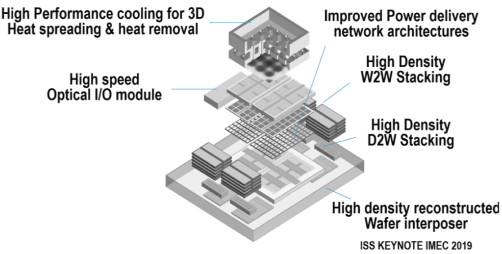
Figure 1: Key building blocks for 3D heterogenous system integration. (Courtesy Jo de Boeck, imec)
Aki Sekiguchi, Deputy GM at Tokyo Electron’s Corporate Innovation Division, started his presentation with a question, to prepare us for the era of big data: How many Zeros are needed to express a Zeta-byte? Answer: 21. Like imec, Sekiguchi also called for new device architectures and materials better suited for the higher level of integration that will be needed in the future.
Paul Enquist, a prolific inventor, and VP of 3D and R&D at Xperi presented the many benefits direct bond interconnect (DBI®) offers, e.g. room temperature bonding, very low thermal and electrical resistance, production-proven pad-pitch of only 3.7µm and die-to-die interconnect height of practically zero. He also explained why companies deploy DBI hybrid bonding in image sensors, LiDAR systems, 3D NAND, RF switches and other high-density applications.
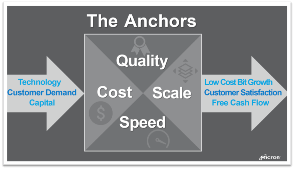
Buddy Nicoson, Sr VP at Micron Technology, walked with us through 50 years of innovation of memory technologies and reminded us that in today’s big data-driven economy, memories are becoming more and more important system building blocks. He listed cost, quality, scale and speed as key success criteria for memory vendors. (Figure 2).
Eric Osby, Research Scientist at Google in Santa Barbara, talked about accelerating computational tasks. He highlighted the need for quantum computing, explained that today’s Qubits show a fairly high failure rate and mentioned the strengths of Google’s Bristlecone chip, utilizing Qubits.
Brian Shieh, VP and GM at Applied Materials’ display and flexible technology division, outlined the state of the art in display technologies. He discussed the transition from LCD to OLED to micro LED displays as well as TVs transition from 4k to 8K pixels. Shieh also mentioned that the first displays projecting true 3-dimensioal pictures are being introduced now.
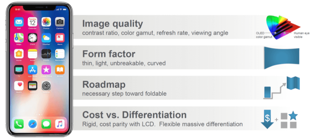
Figure 3: Advantages of OLED displays for mobile phones, (Courtesy of Brian Shieh, Applied Materials)
Industrial Revolution 4.0
Christopher Thomas, partner at McKinsey & Company, is focused on digital and advanced technology. Based on McKinsey’s industry studies, he had a very concerning fact to share with the audience: Only 18% of companies survive a major industry transition.
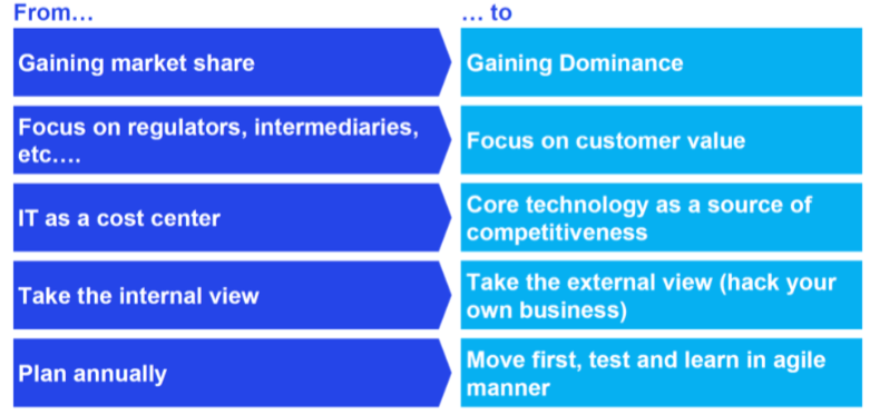
Thomas hinted that the ongoing transition to big data, digital twin, and other efforts towards digitalization of our industry is a major transition and asked for top managements’ attention and commitment to support the necessary changes. He recommended five points, important to successfully navigate a company through such a major transition (Figure 4).
Tim Olson, founder and CTO at DECA Technologies, started his presentation by pointing out another important trend in our industry. The leaders in the traditional “silos” 1) wafer foundry, 2) semiconductor assembly & test and 3) electronic manufacturing services are reaching into each other’s domains, initiating re-integration towards the integrated device manufacturer (IDM) business model.

Then Olson explained DECA’s core technology: adaptive patterning, implemented in and production-proven with their M-Series IC packaging technology.
Because in surface mount technologies die-placement on substrates or re-constituted wafers varies and can lead to yield loss, DECA developed processing steps for adaptive placement and adaptive routing, to compensate for variabilities and improve manufacturing yield significantly. DECA is rolling out this technology, on a large scale, in close cooperation with ASE.
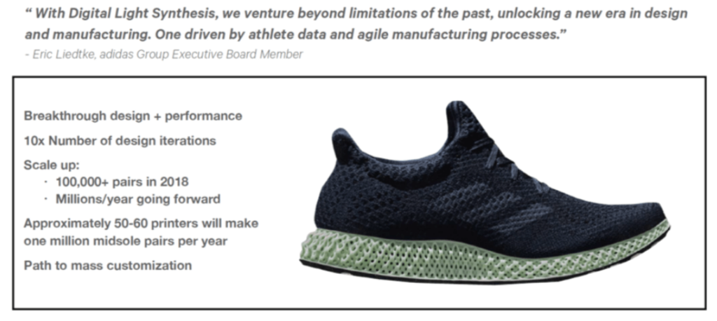
Joseph M. DeSimone, CEO, and Co-Founder of Carbon, presented a compelling application for their digital light synthesis technology. Carbon’s capabilities supersede traditional manufacturing methods. Software-driven design and manufacturing enable Carbon to create a durable and comfortable mid-sole design for Adidas. (Figure 6).

Workforce Development and other Strategic Focal Points
Day three of ISS started with a presentation from Leslie Tugman, VP Workforce Development, Diversity & Inclusion, at SEMI. She drives programs to encouraging young talent to join our industry, on-the-job training and certification programs as well as retraining of returning workers, e.g. veterans.
Marco Chisari, Managing Director at Bank of America Merrill Lynch, stated that in the U.S.during the last 15 years, only 1% of VC investments went into technology and semiconductors. Out of 176 unicorns, there is only one semiconductor unicorn – Graphcore®. In the last seven years only four semiconductor companies – Ambarella, Quantenna, Impinj and Aquantia – were able to go public. In contrast, Chinese VCs invested $ 3.5 B in Chinese semiconductor startups from 2014 to ’18, at a CAGR of 27%. Chisari listed several reasons why the U.S. offer so little support to semiconductor startups. He suggested that VCs, corporate venture funds and governments should recognize the magnitude and implications of this problem and evaluate possible solutions for start-ups, e.g.: Would lower EDA, IP or fabrication cost help? Do they need new growth opportunities or different business models?
James Talent, former U.S. Senator and Republican from Missouri, delivered the closing keynote, focused on the U.S./China strategic relationship. He showed how rapidly China’s military force expanded since the beginning of this millennium, pointed out that this is changing the norm-based international system, as China strives for dominance in Asia. Today, 40 – 45% of China’s economy is controlled by local or the global government. Talent predicted that the next major international conflict will be fought as cyber-war or in space and recommended to deter China – without provoking the country.
After this sobering message, Dan Hutcheson, Chairman, and CEO of VLSI Research, started a panel discussion titled: “The Next Semiconductor Revolution; Filling the Gap between Smart Speakers and Autonomous Vehicles”.
The panelists comprised four industry luminaries: Federico Faggin, design manager for Intel’s first microprocessor (4004), Terry Brewer, President & Founder of Brewer Science, Sanjay Natarajan, Corp. VP at AMAT and Michael Mayberry, CTO, SVP and GM Technology Development at Intel.
Following the moderator’s question of how artificial intelligence (AI) will impact our industry, Faggin started the discussion by stating that our expectations for AI are too high. Brewer highlighted that AI will be very useful in manufacturing to identify defects and improve quality. Natarajan pointed out that we enjoyed following Moore’s Law for too long and need to extend it with More than Moore now, to improve the compute power and energy efficiency as well as reduce variability.
Mayberry warned that it’s very hard to extract an expert’s knowledge and feed it into an AI system. The panelists projected, depending on the specific application, it may take less than 4 years and up to 20 years, when it can benefit from AI.
In summary
ISS 2019 was a very impressive symposium and clearly focused on important and strategic topics. Many manufacturing supply chain experts impressed the audience with their domain knowledge, ideas, and suggestions.
If I may make one suggestion for ISS 2020: Adding a few EDA domain experts as speakers and/or panelists will enable next year’s ISS to truly convey 20/20 vision.
Thanks for following this long blog. I hope to meet you again at ISS 2020 and other occasions. ~ Herb