


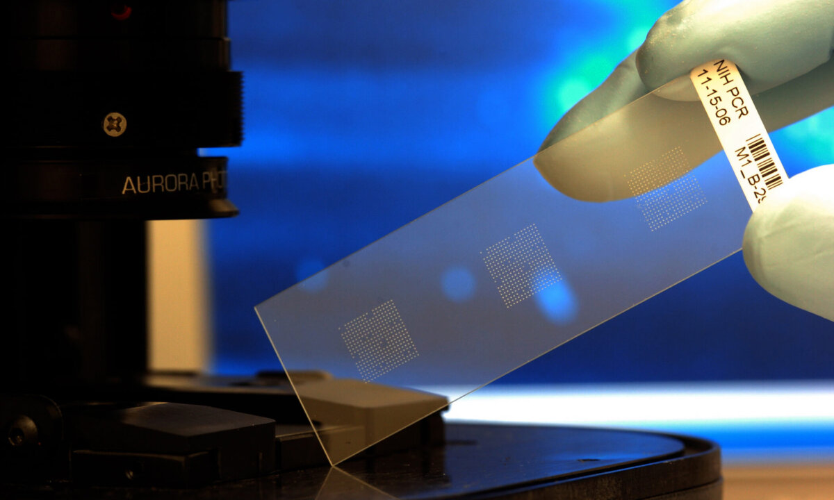
A few weeks ago, Tezzaron announced its latest industry first: an eight-layer 3D IC wafer stack containing active logic, built at its fab, Novati Technologies, a global nanotechnology development center located in Austin, TX. Novati is clearly on a roll, because today they added another industry first to their product portfolio: an integrated sensor platform that is the culmination of everything Novati does: using all the building blocks in its technology arsenal to create new and unique sensor modules to enable the Internet of Things.
I spoke with Dave Anderson, president and CEO, Novati Technologies, to learn a bit more about this platform, and what makes it entirely unique to the industry. Novati will showcase this achievement at SEMICON Europa, which takes place October 6-8, 2015 in Dresden, Germany.
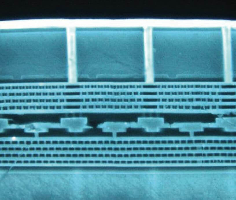
The foundation of Novati’s manufacturing process is wafer-to-wafer integration using Tezzaron’s approach of stacking and bonding layers of circuitry using Ziptronix DBI™ hybrid bonding to achieve high density interconnects. They have extended this capability beyond standard CMOS, and have been successful using the same building blocks to integrate different functionalities, such as image sensing, silicon photonics, and microfluidics; as well as dissimilar III-V materials such as gallium nitride, indium phosphide, gallium arsenide, and quartz.
According to Anderson, with this platform it is now possible to monolithically stack digital, logic, analog, RF, memory, and multiple sensors in one device – something that could previously be achieved using multi-chip system-in-package (SiP) approaches to form interconnects through the package structure. “What we’re doing is eliminating the parasitics of wire bonds and solder joints,” he said. “We build a monolithic stack that is thinned and bonded to each other to build a singular device.”
What makes Novati and its approach unique in the industry is its materials process capability, which allows them to rapidly try out new materials and determine the different effects the properties have on one another, explained Anderson. “We regularly work with more than 60 elements of the periodic table in our fab,” he said. “Traditional fabs typically only utilize 20.” While Novati doesn’t design devices, they work jointly with customers to maximize the efficacy of the design. They are able to develop devices from concept and run low volumes until a high volume is needed.
By nature, the focus of Novati’s devices is performance, and most target low-volume applications. “We’ve done quite a bit of work in the life science and point-of-care diagnostics space,” Anderson noted. “For example, we get brilliant scientists who understand biochemistry coming to us asking for help to build a structure. We recommend alternative materials that may improve the device performance and sensing capability.”
Anderson said that they’ve been working towards this platform for a while through custom customer projects. “We’ve done lots of work in image sensors, and in life science applications, for example DNA sequencing,” he noted. “We came to the realization that what we’re doing has a broader applicability than with a single customer.” Essentially, the platform offers an associated set of building blocks for integration of sensors with other multifunctional layers.

Some examples Anderson described include building a microfluidics MEMS device on top of CMOS to utilize the fluidics channel. They’ve also coupled a III-V sensor with an analog layer and a logic layer for data processing, with RDL layers in between. They can also accommodate differing wafer diameters using die-to-wafer bonding prior to dicing the full stack. They’ve dropped a III-V component into a cavity on a CMOS wafer. The goal, he said, is always to increase performance in a smaller footprint. “We’ve achieved performance characteristics 4X that of the same device built using traditional packaging approaches,” he said.
But don’t expect this to come with a low price tag, at least for the moment. Initially, Novati is targeting security, defense, and medical device/life science applications, which tend to be performance-driven, and less about cost. Once the technology is proven and more prolific, customers will consider the overall system packaging cost, which will be reduced due to the elimination of wire bond, package, and board. Then it will be viewed as a cost-effective solution with high performance benefits. Anderson explained that the platform allows them to take whatever approaches are appropriate – Tezzaron’s stacking, Ziptronix DBI, or through silicon vias (TSV) – to achieve the best performance at the lowest cost for the customer.
As previously mentioned, Novati has selected SEMICON Europa as the venue to launch this new platform. “Europe is a center of innovation. We already have European customers, and there’s room for expansion there,” said Anderson. As such, the company is exploring locations to open an office and business development center to tap into European investment dollars. ~ F.v.T.


