


 Chalk up another industry first for Tezzaron Semiconductor, who announced just today (or tomorrow, if you are there for the excitement at IEEE 3DIC in Sendai, Japan) that along with their manufacturing subsidiary, Novati Technologies, they have successfully manufactured the world’s first eight-layer 3D IC wafer stack containing active logic. (Figure 1). According to Tezzaron, the logic-on-logic stack represents the densest 3D IC ever reported. And they built it in a manufacturing facility, not a lab. This folks, is big news for 3D integration; Really big.
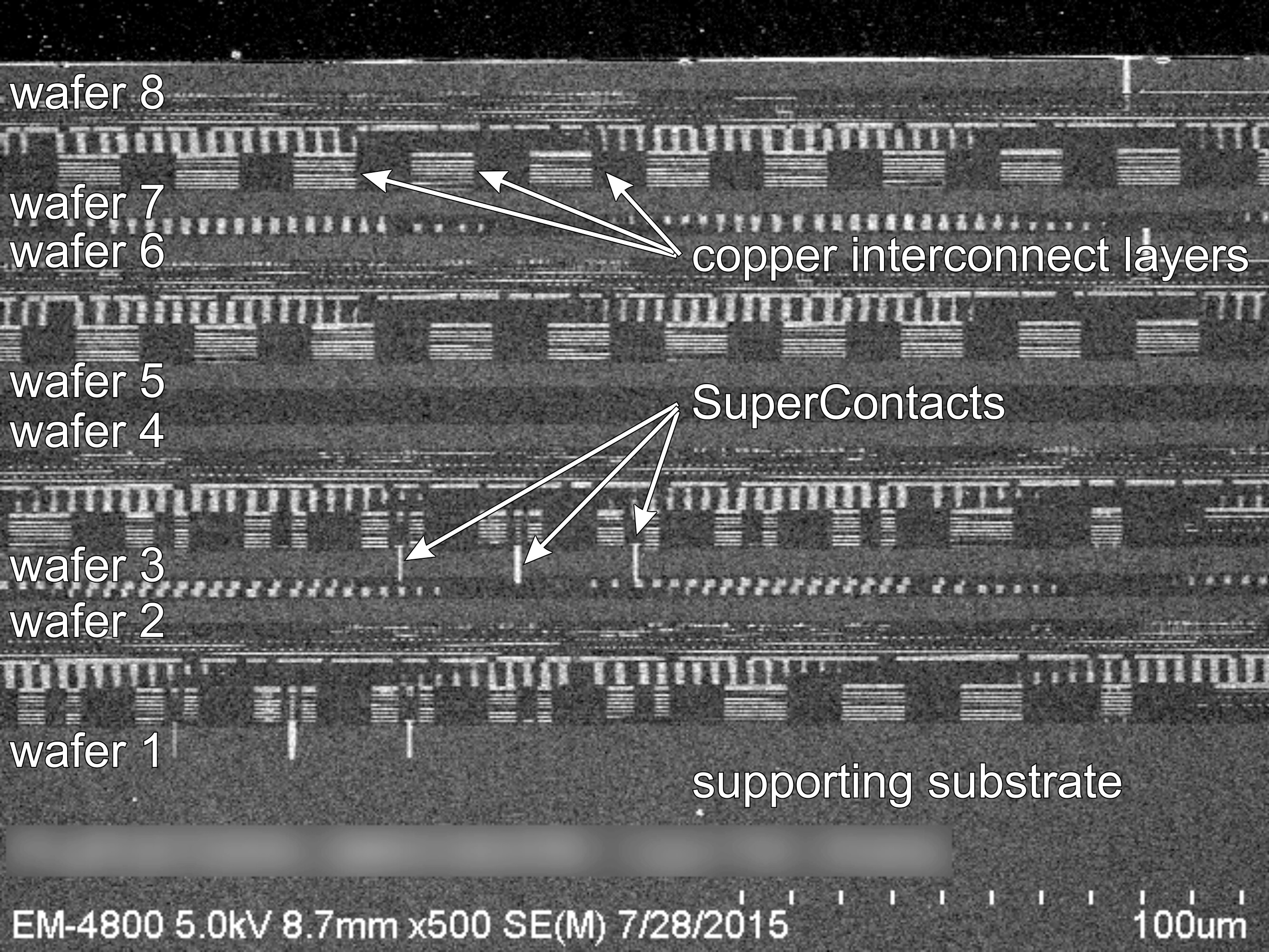
According to Bob Patti, CTO Tezzaron, the target application for this 3D stacked logic device is high performance computing. Each wafer in the stack has 10 layers of copper interconnect supporting high performance CMOS logic, for a total of 80 layers of interconnect and 8 layers of transistors in a finished stack as thin as a single conventional die.
The technologic significance of this achievement is that the transistor and interconnect densities per cubic mm are far higher than achievable with 2D 14nm silicon fabrication, promising to accelerate high-performance computing and put Moore’s Law back on track. The economic significance is that it could potentially save the industry billions of dollars.
“This is well beyond what anyone else can do either in 3D or in 2D equivalent technology,” said Patti.
How did they do it?
While this isn’t the first time Tezzaron has successfully stacked logic-on-logic — according to Patti the first time they did that was in 2004 — this the first time that wafer-on-wafer stacking with logic has reached 8 layers.
So as to not confuse Tezzaron’s design and fabrication approach with others you’ve read about, it’s important to remember that this is not a 3D packaging technology that uses through silicon via (TSV) technology to stack 2D dies into 3D IC assemblies.
Tezzaron’s approach is quite different: There are no wire bonds, copper pillars, bumps, or underfill between the layers. Rather, the 8-wafer stack contains active CMOS circuitry and tungsten vertical interconnects (SuperContacts™). Wafers are 20µm thick; SuperContacts are 1.2µm diameter, 6µm deep, and can be deployed at a pitch of 2.4µm and require no keep out zones near active transistors.
Patti explained that unlike traditional Cu TSVs, SuperContacts are more like a contact than a via as they don’t pierce the whole wafer, just from the bottom layer of metal to the outside (6µm or so). As such, the densities can exceed 170,000 vertical connections per mm². Tezzaron claims that this is 350× denser than state-of-the-art copper TSV vertical interconnect.
Wafers are bonded directly, wafer-to-wafer, using DBI® hybrid bonding, invented by Ziptronix and now available from Tessera. (Tezzaron/Novati was the first licensee of DBI Hybrid Bonding for 3D memory applications, and also acquired Ziptronix applications lab in 2013)

DBI is a conductor/dielectric bonding technology that includes a variety of metal/oxide/nitride combinations, uses no adhesives and is CMOS foundry compatible. Unlike traditional thermocompression bonding that bonds only at the conductor, DBI bonds occur at both the conductive and dielectric materials, allowing the bond to form over the entire surface area, eliminating the need for underfill as well as significantly reducing the overall height of the structure. This produces devices that can be finished to the same thickness as conventional 2D dies. Each wafer in the finished stack is only 20μm thick. This allows vertical interconnects through the stack to be extremely dense and electrically unobtrusive, capable of carrying very small and fast signals.
Paul Enquist, formerly CTO, Ziptronix and now VP at Tessera, cites this as a milestone for DBI as well, as it demonstrates its capability to “achieve transistor scale 3D interconnect pitch with Tezzaron’s SuperContact™ technology, which we believe has an iterative capability beyond eight layers.”
“The extravagant interconnect is very significant,” says Bob Patti. “We can completely reconfigure any circuit and integrate it tightly in all three dimensions for superior performance at one-tenth the power.”
But is it costly to manufacture? “The first one always is!” noted Patti. “Production costs are reasonable for the high performance computing market. We do expect significant cost reductions over the next couple of years.”
Developed as a demonstrator, Patti said the 8-layer logic stack won’t be sold as a product, but is related to one. “We built this device to ‘practice’ for one of our products that will be sold next year,” he said.
So hats off to Tezzaron once again, for leading the way for 3D integration. Is it any wonder Bob won the 2015 3D InCites Individual Achievement award? Just maybe we will see this device in the line up for next year’s 3D InCites Award Device category. ~ F.v.T.


