


After more than a year of touting the turnkey model, even TSMC is jumping on board the collaboration bandwagon for manufacturing 2.5D and 3D ICs at high volume. This revelation came this week at ECTC 2013 (May 28-31, Las Vegas) from TSMC’s Jerry Tzou, who was a panelist during the special session, “The Role of Wafer Foundries in Next –Gen Packaging.”
Chaired by Sam Karikalan, Broadcom, the panel included industry leaders Dave McCann of GLOBALFOUNDRIES, Kurt Huang, UMC, Jon Casey, IBM Corp., and Sudipto Roy, Ph.D SMIC. Each speaker had the opportunity to update us on their company’s roadmaps for 2.5D and 3D ICs before fielding both prepared questions from Karikalan and ad hoc questions from the audience.
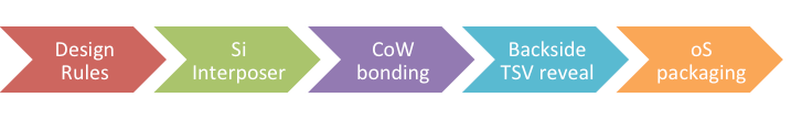
Tzou started things off with an update on TSMC’s activities in 2.5D and 3D, and in particular the much talked-about chip on wafer on substrate (CoWoS) technology, which integrates multiple chips into a single package using a sub-micron scale interface. He said TSMC has developed “a well integrated flow for high yield and reliability to enable higher performance and lower power.” Describing CoWoS as “a three-story house” he explained the construction as a microbumped top die connected to an interposer using through silicon vias (TSVs) which is connected by C4 bumps on the substrate. “Yield is the name of the game for building a three story house, especially when it’s module to module,” said Tzou. He shared TSMC’s process integration flow (Figure 1).
“CoWoS is in production today – it’s not a mystery anymore. We’re shipping products to customers in production volumes at 28nm and below,” said Tzou, adding that they are achieving 95% in-house yield.
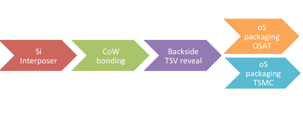
Tzou also announced that TSMC has successfully integrated 3rd party Wide I/O DRAM designed with the CoWoS reference flow and validated at a high-speed memory interface. As such, the company has expanded its service direction (Figure 2) and will now collaborate with customers to design a supply chain model that may or may not integrate OSATS into the supply chain.
Last year, TSMCs story was that they are experienced in copper end-to-end, and so it made sense for them to develop an end-to-end business model. The reasoning was that they would own the liability. How they would integrate third party memory was always in question. So hearing that they support collaboration with OSATS was a big surprise.
Why the sudden change? Tzou explained that currently TSMC is capable of production volume for CoWoS, but as customer requirements increase and the infrastructure is in place and makes sense, it may be more cost-effective to collaborate with OSAT partners. “It’s the model we are used, to be honest, but it was critical to understand all the elements involved and have the capability in house,” explained Tzou. “We couldn’t have understood how all the elements play and what the final product looks like without doing it ourselves.”
Next up was Dave McCann, who declared, “silicon is the package” and talked about disaggregation, saying that SoC scaling is not delivering the full entitlement of cost/area improvement. “SoC Fission” enables overall system level savings. He also noted that reliability in new package technology requires working with customers to understand what application barriers are, understand drivers and the price point.
“You can’t define the silicon solution without considering the packaging solution and understanding the impact to silicon interconnects,” he said.
He reiterated GLOBALFOUNDRIES dedication to an open supply chain collaboration that involves the logic foundry, memory foundry, OSAT and customer. According to McCann, supply chain interdependencies for 3D integration includes the impact of packaging on TSVs and transistors, impact of thinning, designs rules for supply chain yields, definition of yield loss ownership, and 2.5D interposer supply.
“Yield is everything. Yield is the enabler of cost,” said McCann. “You drive adoption by driving yield, which drives cost.”
Both Huang and Roy offered similar opening comments as McCann with regard to their respective companies supporting open collaboration models. Roy pointed out that historically; the industry approach was focused on competition rather than collaboration. “The time has come when we have to understand that we can only compete WHEN we collaborate,” he said

At UMC, noted Huang, various work models are distinguished by who owns the middle-end-of-line (MEOL) processes. UMC does not handle MEOL, but prefers to work with OSAT partners. He said UMC boasts the “world’s first dedicated 2.5D through silicon interposer (TSI) foundry under an open eco-system. The company has an aggressive ramp: 1K wafers/month now with 14K/month expected by 2015. Additionally, he said UMC has achieved the world’s first 3D IC developed under an open ecosystem, with UMC providing 28nm TSV front-end-of-line (FEOL) and STATS ChipPAC providing MEOL and back-end-of-line (BEOL) processes for Wide I/O memory on logic. According to Huang, package-level reliability is successful.
IBM’s Jon Casey provided the only IDM perspective on the panel, and said that we’ve reached the “perfect storm” and that packaging technologies offer the key to survival. What drives this is not the mobile devices themselves, but data.
“Data comes in in lots of ways, sizes and speeds. We have to be able to analyze the data and figure out how to handle it,” explained Casey. “We have to change the way we look at the IT industry.” By way of explanation, he said we need to move compute capability to the data instead of vice versa. “It’s time to change form CPU-centric computing to memory-centric computing,” he said. The key is what he calls ‘volumetric scaling’ which incorporates heterogeneous integration with 3D integration and requires co-development of silicon and packaging solutions that ultimately provides lower cost solutions that enable system performance.
The Q&A segment of the program provided some ‘a-ha!’ moments as well. In answer to the question: what does the semiconductor industry need to focus on to bring down the cost of 2.5D and 3D packaging?, Casey suggested changing the metric to cost/performance to come up with a solution. “The silicon only approach is extremely expensive, which leaves leeway for inducing added packaging cost because the benchmark is high,” he explained. “When we put our packaging hats on, 3D integration adds lots of different steps, but look at the alternative which is an EUV tool. Is it better to spend a few million dollars on a tool that depreciates quickly and you move a few thousand wafers through it?”
Tzou talked about the complexity of integrating multiple technology nodes and materials from different suppliers. “Each of us needs to lower the cost of the module we’re developing, then take the cost of integration into the picture,” he advised.
McCann recommended opening lines of communication with the architecture guys to find enabling price/performance points. Huang says we need to examine system architecture and how to reuse blocks. We have to plan cost down over the next few years.
In other words, from a system-level perspective, integrating 2.5D and 3D ICs reduces cost. From the foundry perspective, there is a cost savings over continued scaling, while from the purely OSAT perspective, its more expensive than some legacy and new non-TSV approaches. Basically, the customer needs to recognize that paying more at the OSAT will save them in the long run.
On the ultimate question of what business model will emerge as the big winner, there was overwhelming consensus among the panel that there are pros and cons to each model, and ultimately all will co-exist, In the end it’s the customer who will decide. “All models will be a winner,” said Tzou. “The customers do have a say. Depending on the technology and what makes sense, there’s no single answer.”
So there you have it. The semiconductor industry is really no different than the rest of the world. At the end of the day, the customer is always right. ~ F.v.T.


