


3D stacking is “already old hand”; or so declared Brion Keller, Cadence, in his keynote talk at last week’s 5th Annual 3D Test Workshop, which took place in Seattle, October 23-24, 2014. In his presentation, 3D Rock from the Sun, Keller talked about the wonders of technological progress, and how we are pulled in the direction of 3D integration because there are products that will have no other way to exist without it.
Keller enumerated the products that are implementing 3D, including images sensors stacked on processor chips and recent announcements about stacked memory products such as Samsung’s VNAND, its DDR4 with 3D TSVs, Micron’s Hybrid Memory Cube, and AMD’s work with SK hynix to explore high bandwidth memory (HBM). he also referenced nVidia’s pursuit of stacked memory integrated with a GPU in an interposer package. Pascal was announced last March at the nVidia annual GPU conference. In this configuration, the GPU is surrounded by four memory stacks (stacked with TSVs). Production is targeted for March 2016.
The stage firmly set for the reality of 3D stacking, discussion throughout the remainder of the workshop turned to the matter at hand: when, how, and why do we test these things?
3D IC Test Standards Update
Imec’s Erik Jan Marinissen, chair of the IEEE P1838 Working Group, led a panel discussion on working group’s progress, which has been significant in define=ing a standardized 3D design for test (3D DfT) architecture for (scan) testing of 3D-SiCs.
The working group has been divided into 3 “Tiger Teams” that work on defining standards for serial control, die wrapper register, and parallel port, respectively. For example, the serial control Tiger Team is working to standardize test access though a serial IEEE 1149.1 test access point (TAP) interface. “Every die should have a TAP,” noted Adam Cron, Synopsys, vice chair of the P1838 Working Group. He explained that there is debate as to whether the standard should be die-centric or stack-centric. His theory is that if the die is standard compliant than the whole stack will be.
Tiger Team 2, focused on the Die Wrapper Register is working to define controllability and observability at the die boundary. Tiger Team 3 is charged with defining a flexible parallel port to allow multi-bit test access for high bandwidth. More details on P1838 progress is available here.
Stacked Memory, What is it and how do we test It?
Vertical memory comes in several flavors, and Betty Prince kicked off the panel discussion on testing memory stacks by first defining the different types and their level of development (Figure 1).
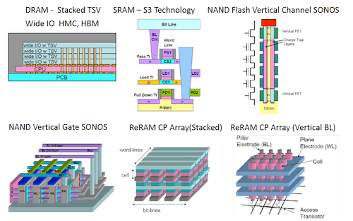
She said DRAM “multi chip packages” (MCP) that are TSV stacked system chips will be in production early in 2015. These include HBM, HMC and Wide I/O. S3 SRAM involved stacked epi layers, and their production date is still undetermined. Vertical Channel NAND flash (like Samsung’s VNAND) will go into early production 2015-2016. Vertical Gate NAND flash is at the prototype stage. RRAM stacked cross point arrays are in 1st layer prototype stage, and lab prototypes for RRAM cross-point arrays (vertical BL) might be available in 2017. The point is, all new memory applications are vertically integrated.
How to test memory stacks focused on those containing TSVs. The best way to achieve this, the panel concurred, is through built-in self test (BIST) and built-in self repair (BISR). Bob Patti, Tezzaron Semiconductor, explained that Tezzaron’s memory stacks are such high density that they have to fix themselves in the field, otherwise it’s too costly. While Patti acknowledged that Tezzaron’s stacked memory, which is uses very high density tungsten-filled TSVs to interconnect layers of circuitry, is different then the garden variety Cu-filled TSVs used in other types of DRAM stacks, there are still compelling reasons why BIST and BISR is the way to go. He also reports that they have no confirmed failures in TSVs.
The BIST/BISR sentiment was echoed by Gary Fleeman, an industry test expert, and Jonathon E. Colburn, principal DfT Engineer, nVidia, USA. Fleeman also quipped that he “picked a good year not to be an ATE guy,” because when it comes to memory stacks, test is going to be more about BIST and BISR and less about probe testing the devices.
The panelists also agreed that testing early is important for 3D DRAM stacks, because the sooner you can diagnose a problem the better. The memory manufacturers need to have good yield to avoid passing bad parts on to the OSATS and middle partners. Areas needing improvement included contacting micro-bumps. While not everyone agreed, Fleeman said he thinks the bumps will eventually require being contacted.
When it comes to a recommended test flow for 3D stacked memory, everyone agreed that as test is always a cost adder, the minimal amount if testing to maximize profits is the goal.

Testing the Interposer
Jan Vardaman, TechSearch International, led the afternoon panel discussion, 2.5D-SICs: Do We Need to Test the Interposer, and If So, How? Panelists included Said Hamdioui, TU Delft; Gerard John, Amkor Technologies,; Choon-Leong Lou, CEO, STAr Technologies; Amitava Majumdar, Xilinx and TM Mak, GLOBALFOUNDRIES; providing representation from across the supply chain.
Mak was the only one to say definitively that we need to test the interposer. “Defects (in TSVs) do happen, no matter how good your process is,” said Mak. He also said while automated optical inspection (AOI) can find defects in the TSV sidewall caused by surface contamination, defects deep in a TSV require a test methodology to discover.
While each of the remaining panelists had different reasons for their opinions, the question of whether or not we need to test the interposer was met with a resounding “It depends.”
Majumdar said that at Xilinx, whether to test the interposer or not is guided by cost, and that the company has a cost model that tells whether or not they should test the interposer. “It’s not emotional, it’s a numbers game,” said Majumdar. “Based on today’s roadmap for interposers and 3D stacked die, it seems for some processes, we should be testing. May be a few years down the road we won’t need to test anymore.”
“Yes to the newbies and no to the oldies” is Amkor’s mantra. Ultimately, noted John, it’s the interposer supplier who is responsible for testing these structures, and that whether Amkor tests incoming parts depends on whether the interposers are coming from known good suppliers, or a company that’s new to manufacturing them. “We’ve built lots of 2.5D ICs at Amkor, and when a part fails, we do a failure analysis. We’ve found the failure is not on the TSV but the microbump,” he sad. He said with new suppliers they test the C4 side, which requires probe cards that aren’t that expensive and are low cost. He also said the company has developed a universal test vehicle for TSV qualification to test the interposers.
Even Leong, the ATE supplier on the panel, agreed that the need to test depends on the application. “We didn’t invest millions of dollars in developing test equipment just to say ‘yes we need to test,’” he joked. When the interposer has reached mass manufacturing and Six Sigma is applied, there’s no need to test. But during development processes, he said test is necessary. STAr Technologies has come up with a tester that integrates parametric, functional, and reliability test. “There are defects that can be seen, and those that can not be seen,” he explained, “Mobile ions and copper migration are impossible to capture by AOI, and it doesn’t tell you about the reliability of the interposer.” He added that in the future, inductors and capacitors will come off the active silicon and become part of the interposer, which will need to be qualified before bringing on the chips.
“Don’t we have to make sure we have a problem that needs to be solve?” asked Bob Patti, from the audience this time. He said when Tezzaron manufactures parts using an interposer; any defects they see aren’t in the interposer but in the assembly.
Since whether to test the interposer does boil down to an “it depends” response, Hamdioui offered a cost model TU Delft developed in collaboration with imec, to determine when it is beneficial to test, and how severe it should be. “If pre-bond test is not feasible, than mid-bond test should be used to reduce overall cost,” he advised. Key parameters to keep in mind included the device application, defect density, yield, fault coverage, test cost and overall cost. “For a mobile applications or FPGAs, if we assume the yield is not 100%, then it makes sense to do midbond testing to end up with lower overall cost,” noted Hamdioui.
After taking in all the different scenarios, here’s what I came away with: at some point in the interposer’s lifetime, it will need to undergo some type of test, and that it is likely to be at the source. The best advice an interposer supplier can take away from this panel is to qualify their products to avoid needless test down the supply chain. ~ F.v.T.


