 For quite some time on 3D InCites, we’ve talked about how breaking up SoC designs into specific functions not only offers a lower cost of ownership than continued scaling, but also allows for heterogeneous integration of disparate technologies that are manufactured at their optimal nodes and then stacked on an interposer or in a 3D IC stack. In fact, these designs are finally being implemented in high-end computing applications – for instance in AMD’s Fiji GPU processor, 22 discrete die manufactured by different companies are integrated into one single package on an interposer using through silicon via (TSV) technology. The challenge that remains is reducing the cost further so that these designs can be implemented in smartphones, tablets, wearables, and other cost-sensitive applications. According to Tim Olson, Founder and CTO of Deca Technologies, the key lies in eliminating the interposer altogether, and using fan-out wafer level packaging (FOWLP) instead. In this Executive Viewpoint, Olson explains Deca’s recent success with building virtual SoCs using its M-Series FOWLP technology.
The Back Story
Initially, Deca put a lot of energy into considering silicon interposers, hoping to leverage the unique equipment, processes ,and operational methods of SunPower, one of Deca’s investors. However, it turned out that cost was less about the silicon and more about TSV fabrication, thinning steps, and creating additional routing layers. “We decided it was going to be too expensive on an area basis for high volume applications,” explained Olson. “So we began to focus our efforts on using a plastic wafer with fan-out technology as the basis for the interposer.” The recent MoChi Architecture developed by Marvell Semiconductor’s co-founder, Chairman and CEO, Sehat Sutardja, and presented at the 2015 ISSCC; is a great example of the possibilities, according to Olson. Starting with single and dual-die applications and growing into virtual SoCs or compete systems modules, M-Series FOWLP technology has the potential to become a direct replacement for what was going to be the Si interposer market in consumer electronics.
FOWLP hits the big time
“The industry loves fan-out,” says Olson, “It’s smaller than anything else next to wafer-level chip scale packages (WLCSP), and it can be low cost and high yielding.” He’s right. Many say FOWLP has become mainstream. Olson credits embedded wafer-level ball grid array (eWLB) technology developed by Infineon and licensed by ASE, STATS ChipPAC, and Nanium with popularizing the idea of FOWLP. Other well-known FOWLP technologies include Freescale’s redistributed chip package (RCP) technology, TSMC’s integrated fan-out (InFO) and Amkor’s silicon wafer integrated fan-out technology (SWIFT).

According to Olson, what differentiates Deca’s M-Series from the other FOWLP technologies available on the market is how it addresses three critical issues that have held back some of the other approaches: Cost of capital for fan-out due to the wafer fab manufacturing infrastructure, die-attach cost due to high precision, expensive and slow tools, and yield due to die-shift and the inability to sufficiently compensate with traditional steppers or scanners. Olson explained how Deca’s M-Series was built from the ground up to address these issues. First, a solar wafer fab inspired Autoline to breakthrough the capital cost barrier, second, use of lower precision, lower cost and fast die placement tools and third, creation of Adaptive Patterning™ technology to adjust for die shift variations on the fly in manufacturing enabling very high yields on par with silicon based WLCSP..
The company’s propriety Adaptive Patterning process solves both the die-attach and yield issues by dynamically adjusting via and RDL patterns using optics and measurement to accurately determine the position and rotation of each die on the panel. This data is then used to create individual package designs that are transferred to a lithography tool to apply a custom, adaptive pattern to each panel. Olson says Deca is already achieving 99.9% yield with M-Series single chip packages through the panelization process. This single chip solution is being implemented on various RF and power management devices, as well as microcontroller and baseband modem chips for smartphones and other applications.
Dual-die fan-out is just the beginning
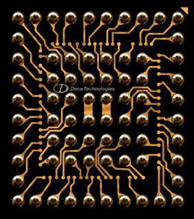
This is where it gets really interesting. Deca’s recent success story is the qualification and planned ramp of a dual-die M-Series for a consumer electronics application. According to Olson, the device integrates two chips with different process technologies (a 28nm ditigal chip and a 130nm integrated RF device) side-by-side in mold compound. The routing goes across the compound connecting the chips as well as fans out to to hold all the I/O for the part. In this way, they’ve constructed an SoC on a plastic panel rather than monolithically on the same piece of silicon. Compared to utilization of existing BGA technology which results in a 10x10mm wire bonded dual-die stacked package, the dual-die M-Series is 59% smaller in footprint and 76% smaller volumetrically. The company also has a multi-die version of this virtual SoC configuration in qualifications, and expects to go into high volume production next year (2016.)
According to Olson, wearables manufacturers will soon look for entire modules that integrate the processor, memory, sensors, and also connect the battery and display. The third phase of Deca’s FOWLP will be such a module, where the processor and memory may be connected laterally or through vias in the mold structure, while the build-up layers on the active sides of the chips can be utilized to surface mount passives, WLCSPs, and other components. The motherboard is eliminated, as well as solder balls: there is no need for BGA interconnects in wearable devices, just connector interfaces.
Olson explained that while other FOWLP technologies have also demonstrated multi-chip configurations, the yield challenges with single chips due to die shift are only exacerbated in multi-chip versions. Additionally, in most instances,the surface structure is not planar. Deca’s adaptive patterning combined with the M-Series face-up planar structure addresses both these issues. Olson says they’ve achieved 5µm l/s with firm plans to take it to 2µm l/s and fundamentally could go lower. “We don’t see customer demand for that right now, “ he noted. “We’re following the technology roadmap to make sure there are customer opportunities.”
Displacing the Si interposer
While it will never replace true 3D IC stacks, Olson says he is confident that this technology can replace a large share of what was to be the Si interposer market and bring virtual SOCs to consumer products. Chips can be wired together the same way as on an interposer, and Cu interconnects can be made through the mold compound at a much lower cost than TSVs in Si. “I see this technology as being capable of 50% lower cost (than Si interposers),” he said. Si interposers will be reserved for the highest value piece – such as in extreme gaming and high-end servers.
In Olson’s vision for Deca’s future, he sees the company becoming “the TSMC of tomorrow “for what we’ll do with chips embedded in plastic combined with high density Cu interconnect. “We’ll be able to build SoCs for companies on disparate pieces of silicon so they can optimize each IP block for a specific technology node,” he said.”We have the building blocks already established. It’s just a matter of time until the IC designers and system architects start adopting the technology for their next-generation of devices.”
If you want to learn more about the future of FOWLP, be sure to attend the panel session, Fan-Out WLP Panel Processing: Will it Happen and What Will it Be? which takes place during on Tuesday, October 13, during IWLPC 2015 in San Jose, CA. Moderated by Jan Vardaman, TechSearch International, Inc, the panelists include Tim Olson, Deca Technologies; Jose Campos, NANIUM, S.A.; Bill Chen, ASE; Beth Keser, Ph.D., Qualcomm; Thomas Uhrmann, EV Group; and Curtis Zwenger, Amkor Technology. ~ FvT


