


I’m not sure what it is about SEMI events held in the U.S. Northeast, but the last two I attended, ASMC 2015 (Saratoga Springs, NY), and the recent SEMI Northeast Forum on Power Electronics Manufacturing (Albany, NY), both reached full attendance capacity before they went live.
Word must be out on the great things happening in New York State.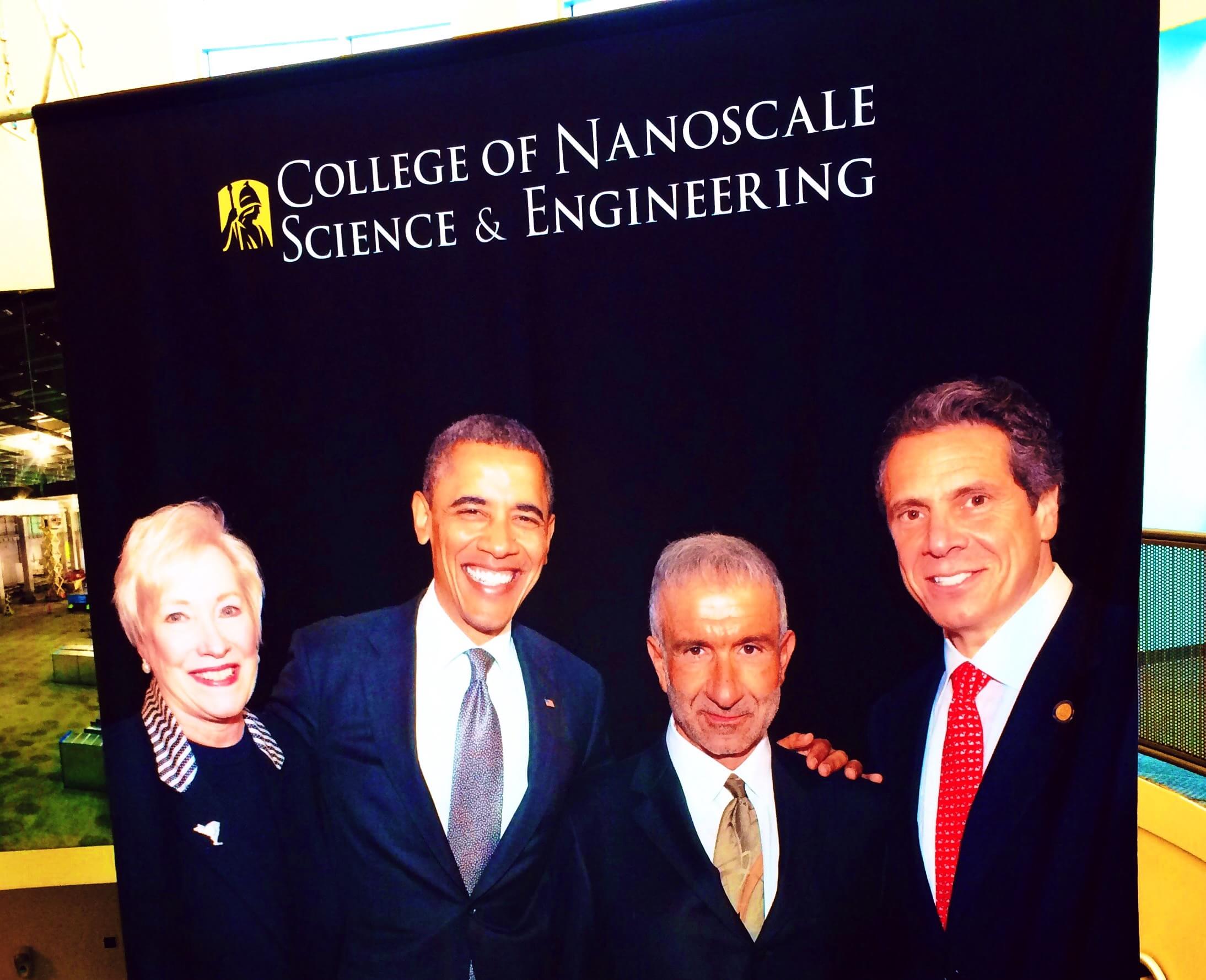
It certainly looks that way in the parking lot at SUNY Polytechnic Institute’s Colleges of Nanoscale Science and Engineering (SUNY Poly CNSE), where I left my car somewhere in the back forty, umbrella-less and coatless in the Autumn rain (the soaker everyone had been hoping for), puddle-hopping around the NanoTech Complex, wishing for my brolly and my Wellies.
Undeterred by the weather, and/or better dressed for it than I was, the audience who filled the room in the CNSE South Rotunda on September 30, 2015 heard from five speakers presenting on the topic of power electronics manufacturing in a program that flowed from the big picture (Paul Farrar, GM, New York Power Electronics Consortium) through to business focus (Peter Sandvik, Product Manager, SiC Business Unit, GE) all the way to supporting vendors and supply chain (Scott Balaguer, Edwards; Somit Joshi, Veeco; Dr. Fulvio Mazzamuto, SCREEN-LASSE).
Well done Margaret Kindling (SEMI), Deb Rafferty (Applied Seals), and the SEMI Northeast Committee!
In his remarks to the Forum, Paul Farrar explained that The New York Power Electronics Manufacturing Consortium (NT-PEMC) is a public-private partnership that will help, together with founding member GE, develop the next generation of power electronics at SUNY’s 150mm SiC wafer fab.
Why silicon carbide, Paul? Higher maximum operating temperatures than silicon-based power devices, reduced power losses, higher power densities, and more reliable operations in high temperature environments are some of the notable characteristics SiC-based devices offer. The commercial markets where SiC power electronics will likely find welcome homes include hybrid vehicles, medical imaging, aircraft, and renewable energy (solar, wind).
 Details about the PEMC SiC fab at SUNY Poly include these: the active team comprises both GE and CNSE staff members and engineers working to establish a 10,000 to 15,000 wafers-per-year SiC production facility based on 200mm processing equipment configured for 150mm SiC wafers.
Relatively speaking, the feature size / lithography requirements for the SiC process are on the order of 0.25µm; beyond photolithography systems, the tool set includes the usual suspects – RIE, metallization, diffusion furnaces, implant, metrology. Tool orders have already been let, with equipment arriving and being installed now through 1H 2016.
Working silicon carbide is expected to be delivered in 2H 2016.
NY-PEMC is actively accepting new members, New York State is offering generous encouragements to new and expanding businesses, and you are encouraged to participate if you at all see SiC in your future. Which GE certainly does, having already seen silicon carbide in its past.
As Peter Sandvik pointed out, GE has a 20+ year history with SiC-based devices, from SiC photodiodes for UV studies of combustion performed more than 20 years ago to working with 4” SiC wafers to produce power MOSFETs demonstrating stable operation at 200°C. In the markets in which GE sees a SiC future, namely aircraft power systems, wind and PV converters, and electric propulsion, among others, the higher cost of a silicon carbide power device over its silicon brethren is outweighed by balance-of-system benefits.
Among these balance-of-system benefits are the lower system costs and the smaller size and lower weight of SiC-enabled PV inverters as a result of the SiC devices being able to operate at higher voltages, thus allowing for simpler system topologies. The naturally higher efficiency of a SiC-based inverter results in lower operating costs, and the resultant decrease in waste heat, along with the higher operating temperature margin for SiC power electronics, means a lower cost thermal management solution for the inverter.
GE understands that using a somewhat more expensive component, the SiC MOSFET, substantially reduces the PV inverter balance-of-system costs. Everybody wins. It’s better living through technology, as a result of imagination at work, and the same value proposition applies to a wide range of products and markets.
 The electronics industry supply chain corridor in New York State covered by Edwards (now part of the Atlas Copco Group) starts in the west, in Buffalo (Lake Erie), moves on the horizontal (Erie Canal) over to Rochester, Syracuse, and Utica, carries on east until it takes a quick look up at Malta, and then bends south to Albany and Fishkill (Hudson River). Along the way you will collect postcards from the PV industry, photonics, GaN power electronics, nano, SiC power electronics, and CMOS IC.

From 1825, when the Erie Canal first opened, to almost 200 years later, today, the same basic route bargemen plied is still a high-tech corridor.
In New York State, follow the money = follow the water.
Under the “One throat to choke” model, Scott Balaguer’s organization at Edwards operates as the one-stop-shop for abatement systems, vacuum equipment, and pipe-work and temperature management systems, performing both hook-up / installations and long-term warranty and service support.
The ‘Green Mode’ capable pumps and abatement systems allow for reduced utility usage during fab idle periods, saving both money and the earth, in the form of reduced CO2 emissions.
Yield and Productivity are the two major cost drivers of the epitaxial depositions required for both GaN and SiC device fabrication and Veeco is working on both drivers for both materials, as we heard in the presentation given by Somit Joshi.
Just as silicon epitaxial technology went from the batch reactor stage to the single-wafer reactor stage for better device yields, and then to the cluster tool stage for better productivity, so too has epi for GaN and for SiC evolved along the same path.
Throw in Continuous Improvement Projects along the way and you arrive having better uniformity, better run-to-run control, lower particles, higher good wafers out, and lower consumables, which are just the things needed to help reduce manufacturing costs for wide bandgap materials.
Trick question: what is the melting point of SiC?
Answer: SiC has no liquid phase, so it can’t really be said to melt. It’s sublime!
And there’s the trick behind UV laser annealing for SiC manufacturing processes, the subject of Fulvio Mazzamuto’s talk. UV laser annealing of SiC wafers enables crystal defect “repair” and the activation of high dose implants, along with being compatible for BEOL processing, where temperature budgets can be tight. The ultra-fast non-equilibrium laser annealing can produce very high (>3,000°C) localized zones of elevated temperature, and could be one of the new process techniques that will give a boost to SiC device and manufacturing maturity, making it that more competitive with silicon-based power devices.
Great things indeed happening in New York State.
From Santa Clara, CA, thanks for reading. ~PFW


