In July and August schools are closed and many people like to take vacation. Typically nothing major happens during these months. Not this year! It was a lively August, if you consider the recent “adjustments” in the stock markets worldwide as a series of events disrupting the summer doldrums. But I am not here to give you investment advice. So let’s move on to a subject I am more familiar with and that also can make you a lot of money.
The title of this blog indicates that its subject is 3D memory cubes and how they can serve your needs. I would like to offer you pointers to recent announcements about the features and benefits of new 3D memories. A surprisingly large number of major IC vendors used the summer doldrums to tell us about the capabilities of their TSV-interconnected and/or monolithic memory cubes in anticipation of September—when you and your company plan new projects, refine your strategies, and start allocating budgets. Just in case your company isn’t utilizing the benefits of memory cubes yet, I also included pointers to other available memory cubes and to very promising development efforts in this field.
You may have heard that these memory cubes are rather expensive today. For proto-typing quantities I fully agree. Prices for production volumes in one or two years will be much more compelling. Also, consider how finally breaking down the Memory Wall will increase the value—and selling price—of your IC-, board-level or system design.
When you are evaluating the many memory cube alternatives, you’ll find that most interfaces do not allow them to be mounted on a printed circuit board (PCB). The drive strength of the I/Os is weaker, therefore they consume much less power. The bus widths are very wide, therefore they offer much higher bandwidth at lower frequencies and low power compared with packaged ICs on PCBs.
If your package substrate vendor can offer a tight enough routing pitch, you can combine the memory cube with your logic chip(s) and other functions (analog, RF, MEMS,…) inside one IC package. If placing the memory cube directly on the package substrate is not an option, consider using an interposer. Organic, glass, and silicon interposers are available.
Enough introductory considerations; let’s focus on the recently announced and previously introduced memory cubes. The pointers will either lead you to the recent announcements, the vendors’ websites or other relevant info sources:
- Samsung offers TSV-based 3D DDR4 DRAMs, monolithic 3D V-NAND, and has deployed the Wide I/O standard.
- Micron and Samsung formed the Hybrid Memory Cube Consortium (HMCC) and offer the TSV-interconnected Hybrid Memory Cube (HMC).
- SK Hynix offers the TSV-interconnected High Bandwidth Memory (HBM) and has demonstrated its strengths in graphics applications at e.g. Nvidia and AMD.
- Tezzaron Semiconductor offers the 4th generation of its TSV-interconnected DiRAM™ and can refer to many military and commercial design wins.
- HBM as well as the Wide I/O Rev 1 and Rev 2 interfaces have been standardized by JEDEC.
In addition to the above memory cubes, the following companies announced recently major ongoing memory cube development efforts.
- CEA/Leti in France is developing the monolithic CoolCube for stacking heterogeneous functions.
- Toshiba and Sandisk announced their joint development efforts towards a monolithic NAND Flash.
- SK Hynix announced their monolithic NAND Flash.
- Intel and Micron have jointly develop a radically new technology for memory cubes and call it 3D XPoint Memory. They jointly announced this “CrossPoint” cubes in a very recent webcast.
As you can see, the race for a slice of the big 3D memory market is on. (I apologize if I overlooked any one of the many contenders.)
The excellent performance versus power ratio, the high bandwidth, small form-factor, other technical benefits (e.g. better NV memory endurance), and eventually competitive pricing of memory cubes will break down the memory wall in most applications.

If you are an IC designer, you must have noticed that closer co-operation with your in-house, or your partners’ IC packaging experts is becoming more important. If you are an IC packaging expert, you have realized that only the right packaging solution will enable the rapid progress on the die/chip-level to really pay off.
To cooperate better, it’s important for both camps to learn more about the others’ area of expertise. Also, both need to know about the latest developments in IC packaging technology, understand their impact on the IC design process, and get data well beyond what’s on the websites I pointed you to above.
How do you keep up-to-speed with all these new developments in advanced high-performance packaging technologies, ultra-low cost alternatives, characteristics of new materials, chip-package design flows and promising R & D efforts? Here are my recommendations for where you can hear in-depth presentations about latest IC packaging technology, material advances, and progress in IC design tools, while also taking advantage of networking opportunities with design- and manufacturing experts from all continents:
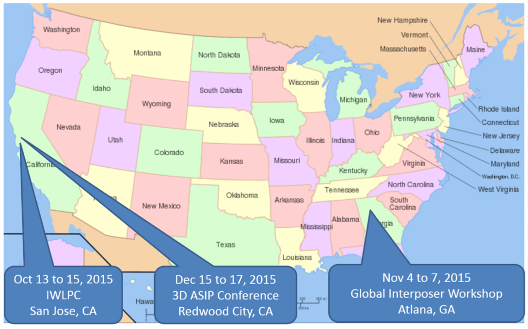
- The International Wafer Level Packaging Conference (IWLPC) begins on Tuesday, October 13, in San Jose, CA. This event is focused on the cost-effective wafer-level packaging technology, as well as interposer-based and vertically stacked 3D-IC designs. Visit the IWLPC website for more information
- The 5th Annual Global Interposer Workshop (GIT 2015) gets underway on Wednesday, November 4, in Atlanta, GA. Organized by the Package Research Center at GeorgiaTech, hundreds of experts in IC manufacturing, IC design and EDA tools meet to update each other… and you. Learn more about the agenda, presenters and how to register for this event.
- The12th Annual Conference on 3D Architectures for Semiconductor Integration and Packaging (3D ASIP) begins on Tuesday, December 15, in Redwood City, CA. See more about agenda, presenters and how to register for this event here.
I look forward to seeing you at all three – or at least one – of these events! ~ Herb