


No SEMICON West would be complete without a few laps around Moscone North and South, and some one-on-one chats with suppliers. I stopped in to see several semiconductor supplier companies who annually request an audience with the Queen of 3D to talk about their latest accomplishments, as well as gain some insight on their perspective of the industry.
I had my 9th annual briefing with Manish Ranjan, who has recently transitioned from Ultratech to LAM Research, where he is now managing director of marketing. We talked about the impact going “beyond 2D” is having on the manufacturing equipment industry.
“It’s clear front-end equipment suppliers are getting serious about the back-end,” he noted, not just because of middle end of line (MEOL) process for 3D, but because packaging — from fan-out wafer level packaging (FOWLP) and system in package (SiP) to interposer integration and die stacking — is becoming a technology enabler, and manufacturing companies are looking for equipment suppliers that can take wafer processes through from the front end to packaging.
“Lam Research clearly views packaging as an inflection growth point in the next few years,” he said, adding that the company has gone rapidly from not having a position to 55+ market share. He attributes this to Lam’s technology differentiation and scale, as well after sales support, process support and an extensive infrastructure.
So what does this mean for equipment companies that have built their business model on supporting wafer level packaging processes from the get-go? Rezwan Latiff, who recently joined Ultratech from TEL-NEXX as general manager and VP of Lithography, says that anything that continues the growth of advanced packaging technologies is good news. He said the advanced packaging market has grown 14-15% year over year, and this spills over into Cu pillar growth. FOWLP is accelerating, this is all good news for Ultratech.
Latiff added that while the entry of front-end equipment companies adds to the competition, the advanced packaging focused equipment companies already have a large install base. “It’s still a cost-driven market, and the front-end guys have some things to tackle; they are competing with a different market and price point,” he said. At the end of the day, the market is customer driven by unit process and cost.
Metrology and Inspection Update
3D InCites has been following Nordson DAGE’s progress with the XM8000 Wafer X-ray Metrology Platform, designed for measuring and capturing defects in wafer bumps and TSVs in interposer integration and 3D ICs. The tool’s initial play has been in detecting voids in wafer bumps, and they have definitely gained some traction in that space. This year, David Bernard, business manager, automated X-ray system was happy to report that they now have real TSV data to show the tool’s capability.
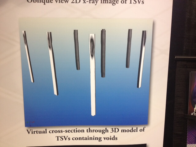
As Bernard explains it, they use a 3D X-ray approach to create a 3D model of the TSV, which takes one second per TSV. They are able to locate the size and position of the voids in the TSVs. Additionally; the images show the full taper and length of the TSVs so you can see the critical dimension (Figure 1).
The benefit of this tool in a volume-manufacturing environment is for process control. “We can catch the void early,” explained Bernard. “The next opportunity to find out something is wrong is after many process steps.” Inspection is performed post-fill, and dies with defects can be eliminated. The tool can also be used for process qualification. “The faster you fill, the greater the propensity for voids, “ said Bernard. “So it can be used to determine how fast you can fill without having voids.” To date, the smallest TSV DAGE has performed the inspection on measures 5×50µm.
Next stop was at Rudolph Technologies, who had several items of news to share. They’ve recently shipped a JetStep Lithography stepper to a “major Taiwanese OSAT” not only for the fan-out wafer level packaging space, noted Rich Rogoff, VP and GM of the Lithography Systems group, but also for Cu pillar and microbumping used in interposer and 3D IC applications. Rogoff says system-in-package (SiP) is also an area of interest for RDL and bumps.
Elvino da Silveira, CTO, Lithography System Group, spoke for the metrology and inspection team, reporting that the company has a system in development that combines inspection and metrology processes (now in two separate tools) into one for 3D macro-inspection of bumps and pillars to evaluate planarity and bump height.
The company’s biggest bits of news were not 3D specific, but applicable in general. With the introduction of the Equipment Sentinel™, an automated fault detection and classification (FDC) software package, Rudolph Technologies has gone into the software business, in addition to lithography and metrology.
The Equipment Sentinal monitors the operating conditions of process tools, looking for abnormalities and implement corrective actions. What differentiates this from other FDC tools is that it also captures information from wafer-level information from an inspection tool to perform predictive defect analysis, and integrates the information from the both tools to find the correlation between tool performance and the wafer. “It establishes trends based on defects to figure out where defects are happening and how they can be prevented,” explained Silveira. “We can stop the process before having to scrap the wafer and fix the process, or the tool, or adjust the tool variations.”

The first implementation of this was done in collaboration with Disco, with the purpose of helping Disco improve it’s saw dicing process. Each tool (the saw and the inspection tool) has a sensor that sends data to the server. The software performs analytics and findings are fed forward with corrections to optimize the tool or optimize the process. This allows for predictive maintenance for the process tool.
For example, understanding how the saw is behaving can predict how to proactively correct the issue. “If a series of defects are detected along cut lines, its an indication of abnormality on the saw. Are these two things related?” explained Silveira. Alternatively, if a flake is made during scribing that could later become a crack, the fault is picked up as a potential fault in the wafer. Instead of performing an inspection of 100% of the wafer, the tool can zero in on that spot to check for a defect. All of this contributes to optimizing the manufacturing process and increasing yield.
Essentially, this software will help in tracking lineage of a chip – from front end fab and follow the wafer all the way through to the OSAT. Information can be handed off between IDMS, Fabs and OSATS, which is the missing link Mike Campbell, Qualcomm, talked about here in the Keynote Panel.
Bonding Update
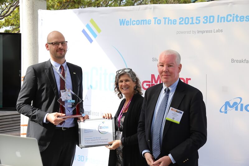 Over at the EV Group booth, the story turned to bonding, and the Gemini GEMINI®FB XT Automated Production Fusion Bonding System, which won the 2015 3D InCites Award for Manufacturing Equipment. Thomas Uhrmann, director of business development, reported positive customer engagements with the tool, and continuous tool improvements to push it to the next node. Plans are to launching a system with a SmartView Aligner for 3 Sigma alignment accuracy to reduce enhance line offset.
Uhrmann says fusion bonding is critical, and there is an end to Moore’s Law (despite what Intel says). Technologies like Leti’s CoolCube monolithic 3D IC application are pushing performance of the fusion bonder, along with the next evolution of image sensors. Uhrmann cited the news that Sony is now stacking DRAM memory on the backside of the image sensor using chip-to-wafer processes.
I asked Paul Lindner, EVG’s executive technology director, if he thinks the recent launch of AMD’s Fiji GPU with HBM was an indication that we were moving into the HVM consumer application space. He pointed out that this particular product was a very high-end GPU, and that serious gaming enthusiasts aren’t fazed by graphics cards that cost $650 or more. (the price of the Radeon Fury with Fiji is reportedly in this ballpark)
“It will be interesting how technology migrates down to lower cost devices and how fast this goes before it gets into disposable consumer products.” he said. “ It’s one thing to provide stacked memory to data center applications where it makes sense to buy more expensive and very fast memory. In consumer applications, power consumption will play a bigger role.”
Lindner predicts a trend away from die-to-wafer stacking towards wafer-to-wafer stacking, as die stacking slows down the process and contributes to lower throughputs. It gets even slower with high accuracy, which will be required as we move toward 5µm die. He says the roadmap is leading to wafer-to-wafer stacking for DRAM, and eventually memory-logic stacking, which will have to be designed to be the same size.
Lindner also says he thinks monolithic 3D IC could beat traditional 3D ICs to consumer applications within the next 3-5 years. “Expensive steps are driven by expensive silicon,” he explained. “Die level stacking is time consuming. Monolithic 3D IC bypasses all the cost errors.”
That pretty much wraps up my supplier interviews. Next up: what’s next in 3D innovation according to imec and Leti, because even though 3D has made it to production, there’s still work to be done, and the R&D guys are on the case. ~ F.v.T.


