Aug 04, 2020 · By Francoise von Trapp · Test and Inspection
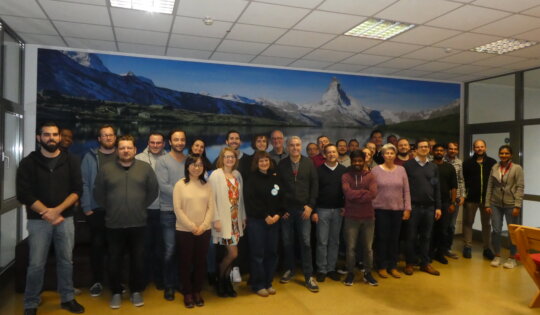
I first met Dr. Thomas Fries, Founder, and CEO of FRT, The Art of Metrology in 2016 at SEMI Europe’s 3D Summit in Grenoble. Fries became a big fan of 3D InCites, following us on social media, and sharing our content. Over the next few years, Fries and the team...Apr 07, 2020 · By Carl Zeiss Microscopy · 3D In-Depth
Much has been written about the end of Dennard Scaling, the slowdown of Moore’s Law and the impact that these events will have on future semiconductor performance and technologies.[1] Much has also been written about semiconductor performance improvements that advanced IC packages are expected to provide that previously resulted from...Mar 19, 2020 · By Francoise von Trapp · 3D In-Depth
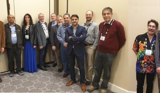
Developing an industry standard is no easy task, and for those involved, its acceptance and publication is something to be celebrated. On March 13, 2020, after eight long years, members of the IEEE 3D-DfT Working Group, from all various corners of the world, sent up a collective cheer to see...Mar 17, 2020 · By Francoise von Trapp · 3D In-Depth
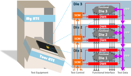
Eight years in the making, the IEEE Std 1838™-2019 Standard for Test Access Architecture for Three-Dimensional Stacked Integrated Circuits — or IEEE 1838, DfT for 3D IC, as it’s known in inner circles – was published on March 13, 2020. Simply put, this standard will allow stacked dies in 3D ICs to connect...May 17, 2019 · By Erik Jan Marinissen · 3D In-Depth
When I joined imec in October 2008 to work on test and design- for- test (DfT) of 3D-stacked integrated circuits (ICs), there were only a few test folks active in that emerging field. Consequently, misconceptions about 3D test were omnipresent. In the November 18, 2008 issue of Semiconductor International, Alexander...Apr 11, 2019 · By Dario Alliata · 3D In-Depth
The expected increase of the power device market, with a compound annual growth rate (CAGR) of more than 10% — and more particularly insulated-gate bipolar transistor (IGBT) products for automotive and other applications — is pushing the semiconductor industry to adopt specific process solutions. The maturity of IGBT market, boosted...Aug 21, 2017 · By Erik Jan Marinissen · 3D In-Depth
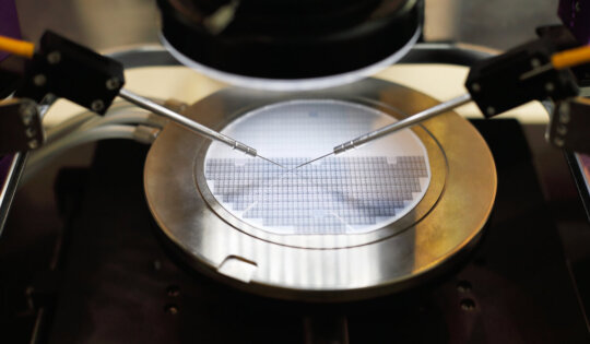
Stacking chips on top of each other (aka 3D stacking) is a well-known approach to make more compact and powerful systems. Until now, it was impossible to probe the large arrays of fine-pitch micro-bumps on advanced chips before stacking. This had a negative effect on the compound yield (because of...Jun 17, 2015 · By Francoise von Trapp · Test and Inspection
As Si interposer and 3D stacked memory devices enter into production, albeit in low volumes, semiconductor manufacturers are lining up their ducks to be ready for high volume manufacturing (HVM) when it happens. As a result, some suppliers of high volume manufacturing equipment who have been rather quiet through the...Mar 19, 2015 · By Francoise von Trapp · Blogs
A second side trip on the way to DATE 2015 brought me back to Nimes, France to check up on activities at Fogale Nanotech since last year. I was reminded once again, that Fogale isn’t just a semiconductor equipment supplier. Its core competencies are optical and capacitive sensing technologies, and thanks to...Oct 29, 2014 · By Francoise von Trapp · 3D Event Coverage
3D stacking is “already old hand”; or so declared Brion Keller, Cadence, in his keynote talk at last week’s 5th Annual 3D Test Workshop, which took place in Seattle, October 23-24, 2014. In his presentation, 3D Rock from the Sun, Keller talked about the wonders of technological progress, and how we...Jun 23, 2014 · By Francoise von Trapp · 3D In-Depth
CIRCL CV310i module is an advanced Wafer Edge inspection, metrology and profiling system tailored for Advanced Wafer Level Packaging. Simultaneous wafer edge inspection and metrology enables comprehensive data collection from all zones comprising the wafer’s edge: top and bottom near-edge; top and bottom bevel; and apex. Testimonial Some of the...May 23, 2014 · By Francoise von Trapp · 3D In-Depth
The TMAP DUAL 3D 300 A is a unique metrology and inspection tool available to the semiconductor industry capable of addressing all customer measurement requirements for MEMS and 3D packaging. The TMAP is highly flexible, accurate, and repeatable. The heart of this tool is based on multi-sensor heads which include...May 12, 2014 · By Francoise von Trapp · 3D In-Depth
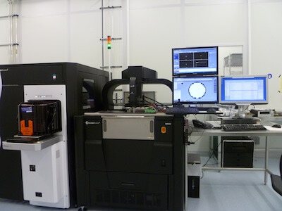
Fully automatic, in-line X-ray metrology platform for the measurement and defect capture of both optically hidden and visible features in wafers and 2.5D/3D IC packages. Available measurements include voiding, via fill, overlay and critical dimensions in TSVs, wafer bumps and MEMS. Testimonial: The XM8000 Wafer Metrology Platform provides a new...Apr 07, 2014 · By Francoise von Trapp · 3D In-Depth
My visit to imec to meet with the Cascade Micorotech and imec 3D Test collaboration team included a tour of the 3D test lab to see the CM300 in action, so we suited up for Class 1000 cleanroom and stepped inside. Generally we would have had to prep for class...Apr 07, 2014 · By Francoise von Trapp · Blogs
For quite some time, the lack of cost-effective test solutions for 2.5D interposers and 3D stacked ICs (3D SICs) has been at the top of many industry experts’ laundry list of ‘what’s-holding-up-commercialization for 3D’. First, there are technology issues: fine-pitch probing, pin count, contact force and the phenomenon of weak...Apr 01, 2014 · By Francoise von Trapp · 3D Event Coverage
The Friday 3D Integration Workshop at DATE 2014 once again found me among friends, as an intimate group of about 30 gathered to spend a day sharing knowledge gained since last year’s workshop. My key take-away for the day was how to achieve reliability and robustness. Jürgen Wolf, director of...Mar 25, 2014 · By Francoise von Trapp · Blogs
In the world of 3D ICs, where features are becoming finer and submicron accuracy and precision is more important than ever to maintain intra-wafer uniformity throughout the wafer or die stacking process flow, process control by means of metrology and inspection is more important than ever. The industry offers a...Mar 07, 2014 · By Francoise von Trapp · 3D In-Depth
Thank you, Ann Steffora Mutschler (Semiconductor Engineering) for getting to the bottom of the difference of EDA tools for 2.5D and 3D IC design and test, and providing such a clear explanation in your post, “Evolution vs. Revolution”. In this 2-part post, Mutschler explores the EDA vendor arguments that “tool...Feb 20, 2014 · By Francoise von Trapp · 3D In-Depth
In Jan Vardaman’s recent readiness report card issued at 3D ASIP in December, 3D IC thermal management issues scored and “F” for lack of a solution o the hot-spot problem when stacking memory on logic. And while she gave 3D IC test a “B” for probe card development, it got an...Jan 08, 2014 · By Bernhard Lorenz · Blogs
Metrology, process control, and electrical test are key enablers for the success of the semiconductor industry. 3D integration using TSVs offers new challenges in this area that need solutions. There seems to be industry consensus that it is extremely difficult to perform a wafer-level test that ensures the complete functionality of...