Mar 23, 2015 · By Paul Werbaneth · 3D In-Depth
In Parts 1 and 2 of this series, I drew your attention to what Peter Clarke, writing in EETimes on 02 January 2015, called the “15-in-15: Analog, MEMS and sensor startups to watch in 2015.” If we were to look for heterointegration spoor amongst Peter’s 15 notable startups what would...Dec 09, 2014 · By Francoise von Trapp · 3D In-Depth
We’ve heard it expressed many times whenever there’s a new interconnect technology vying for adoption: manufacturers will select the best performing option at the lowest cost to do the job. However, as performance requirements reach previously un-anticipated levels, pitch requirements become tighter, and density requirements become higher, the job of...Jun 20, 2014 · By Francoise von Trapp · 3D In-Depth
SSEC’s wet TSV reveal process achieves -/+ 0.7% Si thickness uniformity under the appropriate post grinding conditions with fast throughput. The two-step process starts with a spin etch for a smooth, fast etch at 10µm/min. The etch is stopped 2µm above the TSVs and then finishes with a selective etch...Jun 19, 2014 · By Francoise von Trapp · 3D In-Depth
Akrion Systems’ vacuum prime and drying technology enables the use of a wet immersion method to introduce liquid chemicals or rinse water throughout the entire HAR feature prior to the oxide etching step. Pulling a vacuum below the saturated vapor pressure of water, draws liquid into the entire feature, enabling...Jun 17, 2014 · By Francoise von Trapp · 3D In-Depth
SETNA, in conjunction with Research Triangle Institute (RTI), has developed a binary alloy (Silver-to-Indium) bonding system for 3D IC assembly that can be compression-bonded at room temperature. Following 3D IC chip stacking, the Ag-In structure is annealed in the solid-state (no melting) to form an Ag₂In interconnect which is stable...Jun 06, 2014 · By SPTS Technologies · 3D In-Depth
The blanket silicon etch process performed on the SPTS Rapier XE achieves an etch rate >8.5µm/min, high selectivity (Si:SiO>150:1), and is ~3-4x faster than competing systems. A unique dual plasma source design creates a uniform etch (<±3%) across a 300mm wafer, which can be “tuned” to compensate for variations in in-coming...Jun 02, 2014 · By Francoise von Trapp · 3D In-Depth
SSEC’s WaferEtch™ TSV Revealer is a single wafer wet processing platform for 3D IC and interposer wet etching applications designed to reduce processing and capital equipment costs. The WaferEtch features superior uniformity of silicon thickness (as low as -/+ 0.7%). Testimonial Via reveal is a critical process step in 2.5D...May 23, 2014 · By Francoise von Trapp · Processes and Technology
The BGM300 was designed to enable quick and accurate measurement of Through Si Via (TSV) depths, Si wafer thickness, and Remaining Si Thickness (RST) above TSVs – all essential in a managed backside via reveal process flow. Back grinding errors due to “blind” grinding can lead to significant yield loss....Apr 22, 2014 · By Francoise von Trapp · 3D In-Depth
At the beginning of April, the Semiconductor Industry Association released the 2013 International Roadmap for Semiconductors (ITRS), which has traditionally served as a guide for “assessing and improving the future of semiconductor technology,” according to Brian Toohey, president and CEO, Semiconductor Industry Association. Sponsored by five regions of the world...Apr 16, 2014 · By Francoise von Trapp · 3D In-Depth
As advanced packaging facilities transition their manufacturing from round wafers to square panels, the JetStep S Series Lithography System is fully capable of handling panels up to Gen 3.5 (720x650mm). The system offers high throughput through a large printable exposure and increased productivity through on-the-fly autofocus for thick photoresists. Testimonial...Mar 20, 2014 · By Francoise von Trapp · 3D Event Coverage
At IMAPS DPC 2014, which took place March 11-13, 2014, in Fountain Hills, AZ, there were several presentations focused on new developments in cleans for TSVs and Cu bumps for 2.5D and 3D IC processes. Cleans has become increasingly important as bump pitches are reduced and TSVs have higher aspect...Feb 25, 2014 · By Francoise von Trapp · 3D In-Depth
Every once in a while, it’s important to remember that through silicon vias (TSVs) might not be the only game in town. While many continue to forge ahead, with commercialization so close we can taste it, others are already moving on to the next thing or looking for alternatives. Will...Nov 21, 2013 · By Francoise von Trapp · 3D In-Depth
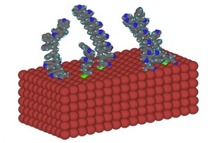
I’ve been on a quest to find out more about EV Group’s new polymer filled TSVs since they first announced it in September. According to a company press release, NanoFill™ process is said to provide “void-free via filling of very deep trenches and high-aspect ratio (HAR) structures, and is suitable...Nov 07, 2013 · By Francoise von Trapp · Blogs
BeSang Inc, a fabless semiconductor company in Beaverton, OR, has been on my 3D IC radar since 2008, when I first edited a 3D technology cover feature in Advanced Packaging Magazine, written by George C. Riley, that included a status report on BeSang’s TRUE 3D ICs™, which had just been...Oct 29, 2013 · By Francoise von Trapp · 3D In-Depth
Did you know that when foundries talk about 14nm and 16nm node chips, these devices are in reality no denser than their 20nm predecessors? Or that a particular node name does not reflect the size of any particular chip feature, as it once did? Or that since 2007, the doubling...Sep 18, 2013 · By Francoise von Trapp · 3D In-Depth
Big news for 3D ICs this week as TSMC and its OIP Ecosystem Partners announce the release of silicon-validated reference flows for both 3D IC stacks and 16nm FinFETS (everyone else puts the 16nm FinFETS first, but I’m most excited about the 3D IC news.) According to Peter Clarke in...Jul 30, 2013 · By Iulia Morariu · Blogs
We have a guest contribution from Zvi Or-Bach, the President and CEO of MonolithIC 3D Inc. Zvi adds information to his previous blog post: Dimension Scaling and the SRAM Bit-Cell. I just downloaded the ASML presentation from Semicon West2013 site – ASML’s NXE Platform Performance and Volume Introduction. Slide #5...Jul 30, 2013 · By Iulia Morariu · Blogs
We have a guest contribution today from Brian Cronquist, MonolithIC 3D Inc.’s VP of Technology & IP. Brian discusses about MonolithIC 3D Inc.’s participation at Semicon West 2013. Thanks to everybody who came by the Silicon Innovation Forum poster session at SEMICON West 2013. We really enjoyed talking with you about...Jul 22, 2013 · By Francoise von Trapp · 3D Event Coverage
Streamlined and versatile: that’s the impression I came away with after talking to Nao Shoda, senior director of business development and technology, Alchimer, about recent developments to further optimize the companies’ electrografting processes for through silicon via (TSV), isolation, barrier, seed and fill steps. I wrote about them frequently in...Jul 22, 2013 · By Francoise von Trapp · 3D Event Coverage
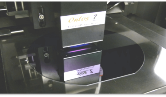
This is part of a series of short interviews, based on face-to-face meetings at SEMICON West 2013. SET is known in the 3D IC world for its high accuracy die bonder for die-to-die and die-to-wafer stacking. The SET Representative in North America (SETNA) has also launched a companion tool, ONTOS7,...