Hybrid bonding enables an assortment of possible chip architectures, mainly targeted at high-end applications including high-performance computing (HPC), artificial intelligence...
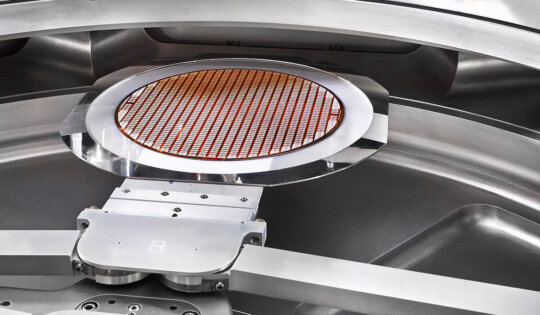
NanoCleave enables Laser Debonding on Silicon with Nanometer Precision In semiconductor manufacturing, 3D integration – the manufacturing, vertical assembly, and...
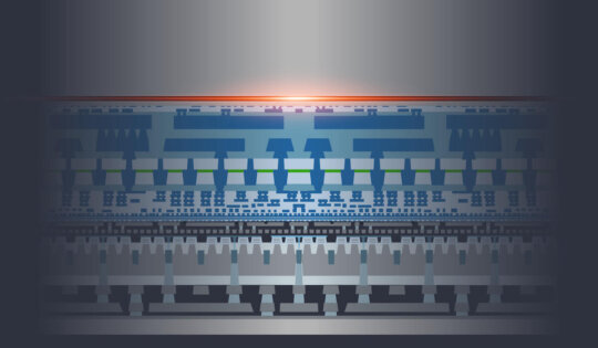
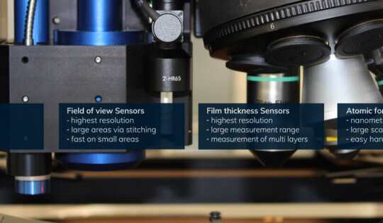
Electronics Packaging vs. Advanced Packaging Electronics packaging is generally divided into three major areas, traditional packaging – also called standard...
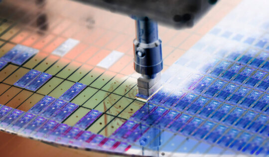
Economics are forcing semiconductor manufacturers away from traditional 3D through silicon via (TSV) packaging integration. The future of advanced packaging...
With each passing year, emerging growth application areas such as Automotive, Cloud Computing, Industrial Automation, and Telecom (5G) Infrastructure are...