


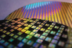
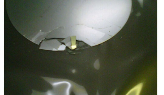
ECTC 2013 Interview: SSEC’s Laura Mauer Talks about TSV Reveal and TSV Clean
This year’s 3D InCites coverage of ECTC 2013 features a series of interviews with suppliers to the 2.5D and 3D IC market. I spoke with a number of exhibiting and attending companies who had progress reports on their tools, processes and materials aimed at leaping over the remaining hurdles. The...
3D Super Chips, 2.5D Technology Advancements, and 3D through the EDA Lens
TSMC calls them 3D Super Chips. The rest of the industry calls it 3D heterogeneous integration. Whatever way you slice it, either 2.5D or 3D IC, it requires TSV technology for its method of interconnect. Here are a few recent items about the latest progress in the march to commercialization...
A Lull in 3D Activity or Stealth Mode?
An industry colleague commented to me recently that the press seems to have lost interest in 3DIC. As probably the industry’s most avid follower and writer of 3D related news, I had to disagree – its not that we’ve lost interest, its just that there seems to be a lull...

3D IC Reality Check
The good news: While forecasted dates for 3D IC volume manufacturing continues to be pushed out, clearly foundries and OSATS are gearing up to be ready when it does. The bad news: Forecasted dates for volume manufacturing of 3D ICs keep being pushed out. Or do they? Rick Merritt, EE Times, posted a...
For Discussion: Is Wright’s Law a better Economic Index for 3D ICs than Moore’s Law?
I just came across a slightly mind-blowing snippet in Forbes Magazine about a study conducted by MIT and Santa Fe Institute comparing the effectiveness of different forecasting methodologies for predicting how rapidly technology will advance. The study concluded that the two most accurate methodologies are the well-known Moore’s Law and lesser-known Wright’s Law. As we all...

2013 Predictions for 3D ICs as reported by SPN
While most of the semiconductor trade publications wrapped up their 2013 prediction posts by mid January, Semiconductor Packaging News (SPN) forged on with its original annual Viewpoints series right up until last week. I spent some time pouring over the musings of industry executives’ contributions. Many discuss the proliferation of mobile...
Proof that the Collaboration Model Works for 3D ICS
For the past year or so at various conferences, symposiums and summits focused on 2.5D and 3DIC technologies; we’ve been hearing suggestions about business model scenarios. It’s boiled down to three distinct choices. First is a ‘single integration’ model where end-to-end manufacturing takes place in one location – most likely...

Alchimer Resurfaces at the European 3D TSV Summit
It had been awhile since I heard from the folks at Alchimer about the progress of electrografting (eG), its “all wet” nanometric film deposition processes. For a while, it seemed like there were exciting things to report every few months, and then POOF – All went dark. So I was...
2013 Predictions for 3D ICs as told by Everyone – Part 1
It’s that time of year again when various electronics trade publications invite industry executives to peer into their crystal balls and make their predictions for the coming year. I’ve been perusing through everything from overall industry forecasts by market analysts to suppliers eager to promote their core competencies for 3D...
Temporary Bond/Debond: Not Ready for 3D TSV Prime TIme
It’s too bad SUSS MicroTec’s Wilfried Bair was one of the last presenters on Friday at 3D Architecures for Systems in Packaging Symposium (3DASIP), Dec. 14, 2012, because more people should have been present to hear what he had to say. While most presenters focused on successes and future work...
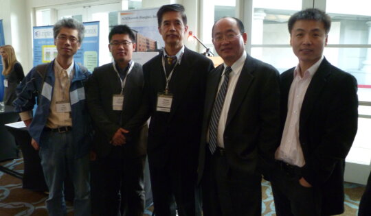
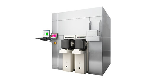
ACM Research: New Kid on the 3D Block
Yesterday at the pre-conference symposium for 3D Architectures for Semiconductor Integration and Packaging (3D ASIP), I was fortunate to get an up close and personal tutorial preview by David Wang, CEO of ACM Research, on the tool manufacturer’s latest process solution for two critical points in the TSV fabrication process. The...
3D Company Updates
There are a couple of notable updates circulating this week involving companies in the 3D space. The first I saw was news from Sony that it has introduced its next-generation CMOS Image sensor they claim is “ the industry’s smallest, CMOS image sensor and camera system”. The image sensor is...
“Known Good Die” has a new name
After 20 years of chasing elusive Known Good Die (KGD) to achieve high yielding advanced interconnect technologies, the semiconductor industry has come to the conclusion that its time to take a different approach. It’s called Probably Good Die, and when it comes to 2.5D and 3D ICs, particularly for Memory,...
Multi-Die Integration Provides Multifaceted Solutions
Multi-Die Integration Provides Multifaceted Solutions By Francoise von Trapp, 3D InCites This year’s Roadmaps for Multi-Die Integration Symposium, hosted by MEPTEC on November 14, 2012 at the Biltmore Hotel in Santa Clara, CA, offered some interesting and different perspectives than the garden-variety 2.5D and 3D IC conferences of late. While...
What 3D Means in eWLB
Last week (November 6) STATS ChipPAC issued a press release announcing that its advanced eWLB provides a platform for 2.5D and 3D technologies. In search of further information about this, I found a feature article recently published in Solid State Technology that explained how eWLB can be leveraged for 2.5D and...
3D Technology Features in Review
The latest digital issues of Chip Scale Review and iMicronews’ 3D Packaging magazines hit the virtual “stands” last week, and perhaps in honor if the 3D ASIP Conference that gets underway later this week, there are some hot new 3D technologies being featured. But first, to bring everyone up to...
Tezzaron, Novati and 3D ICs: They’re doing it in the USA
While everyone’s waiting for the big memory houses like Micron and Samsung, and IDMS and foundries like IBM and TSMC to announce they are ramping to high volume manufacturing (HVM) with 3D ICs, deep in the heart of Texas, it’s already happening in low volumes for custom applications thanks to...
Some 3D Technology Tidbits
Glass interposers got a thumbs up from i-MicroNews in a “Closer Look” post reviewing Corning’s Peter Bocko’s presentation at IMAPS 2012. Based on work done as part of Ga Tech’s consortium, Bocko demonstrated that “glass interposers show less warp during chip assembly, faster signal propagation and significantly reduced signal loss. In...
3DIC Tech Updates
But first, a 3D history lesson thanks to a recent SemiWiki blog post, Hybrids on BeO then, 3D-IC in silicon now, in which blogger Don Dingee recalls lessons learned from working with hybrid microelectronics assemblies, and how they apply in the world of 3D. Calling 3D ICs “the modern version of...
Just another 3D Monday
For me, Mondays are about regrouping, getting out of weekend head and into what’s going on in the 3D world. (I confess, I do leave my work at the office!) Mostly I cruise around looking to be inspired. Here’s what was waiting for me today. Symmetry is an online magazine...