Nov 13, 2013 · By Andrew Walker · Blogs
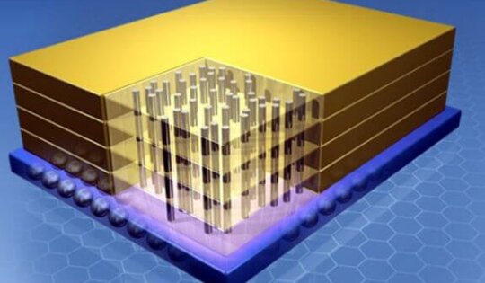
In my last blog posting I went over the cost aspects of the Samsung-Toshiba 3D NAND approaches. The conclusion is quite stark: if those vertical holes and trenches are more than a few tenths of a degree from the vertical, then the whole approach can be undercut in cost by...Oct 29, 2013 · By Francoise von Trapp · 3D In-Depth
Did you know that when foundries talk about 14nm and 16nm node chips, these devices are in reality no denser than their 20nm predecessors? Or that a particular node name does not reflect the size of any particular chip feature, as it once did? Or that since 2007, the doubling...Oct 25, 2013 · By Francoise von Trapp · 3D In-Depth
Word on the street is, New York will soon be known as Nano York, with all the money the state is pouring into nanotechnology research and development. The most recent announcement by Governor Cuomo is a $1.5 Billion Public-Private investment intended to turn the Mohawk Valley (Utica) into the next...Oct 14, 2013 · By Andrew Walker · Blogs
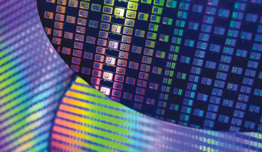
The transition to 3D NAND Flash seems to be imminent with projections of it being half the total NAND Flash market by 2016. That means tens of billions of dollars within 3 years. V-NAND is Samsung’s version. Their first publication describing this architecture was released in 2009 and was called...Sep 18, 2013 · By Francoise von Trapp · 3D In-Depth
Big news for 3D ICs this week as TSMC and its OIP Ecosystem Partners announce the release of silicon-validated reference flows for both 3D IC stacks and 16nm FinFETS (everyone else puts the 16nm FinFETS first, but I’m most excited about the 3D IC news.) According to Peter Clarke in...Aug 23, 2013 · By Francoise von Trapp · 3D In-Depth
There’s been a lot of buzz around 3D NAND in the past few weeks, sparked by Samsung’s recent announcement that it was commercializing its 3D VNAND technology. There’s also been some discussion (mixed with concern) about how, if at all, 3D NAND might affect the commercialization of TSV-based 3D DRAM...Aug 16, 2013 · By Herb Reiter · 3D In Context
At last week’s Memcon 2013, which took place Tuesday, August 6, 2013, at the Santa Clara Convention Center, Keynoter Bob Brennen, Senior VP at Samsung, talked about the need for New DRAM and Flash Memory architectures. Richard Goering summarized Brennan’s keynote very well in his blog post. Because Brennan’s responsibility...Jul 02, 2013 · By Francoise von Trapp · 3D Event Coverage
Subscribers are practically blowing up 3D InCites as they duke it out online and race the July 3rd deadline for casting their ballots in the public opinion poll for this inaugural 3D InCites Awards; which is great because the first 3D InCites Awards Breakfast, co-presented by 3D InCites and TechSearch...Jun 28, 2013 · By Francoise von Trapp · 3D Event Coverage
So SPIL’s offering a turnkey model for 2.5D interposers, including fine-pitch fabrication of the interposer wafers themselves? This is certainly an interesting turn of events, particularly with TSMC’s recent announcement that they’re not married to the turnkey model and are willing to collaborate with OSATS. SST’s Phil Garrou got the...Jun 07, 2013 · By Francoise von Trapp · 3D Event Coverage
The ECTC 2013 stats are in. This year showed increases across the board with: Over 1,300 attendees, the highest attendance ever, from 26 countries 377 technical papers, presented in 36 oral and five interactive presentation sessions, including a student poster session 12 sessions focused on 3D/TSV, including several of the...Jan 04, 2013 · By Francoise von Trapp · 3D In-Depth
I don’t know about you, but I always find that amidst the holiday hubbub, the really important stuff gets shoved aside and falls through the cracks. Just in case you missed them, here are some good 3D related posts that may have been lost in the December race to “get...Dec 10, 2012 · By Francoise von Trapp · 3D Event Coverage
Previews of IEDM 2012, which got underway today in San Francisco, indicate a program this year rich in content on 3D transistors and 3D memory technologies, with very little focus on 3D ICs using TSVs. My take on this is that IEDM papers are generally focuses on processes and technologies...Dec 10, 2012 · By Francoise von Trapp · 3D In-Depth
There are a couple of notable updates circulating this week involving companies in the 3D space. The first I saw was news from Sony that it has introduced its next-generation CMOS Image sensor they claim is “ the industry’s smallest, CMOS image sensor and camera system”. The image sensor is...Nov 27, 2012 · By Francoise von Trapp · 3D In-Depth
Ever since TSMCs Open Innovation Platform (OIP) event, we’ve been hearing all about how the company has qualified its 2.5D chip-on-wafer-on-substrate (CoWoS) process flow, announced its test vehicle, and has begun shipping products. Indeed, at Roadmaps for Multi-die Packaging (November 14, 2012) Jan Vardaman used Altera’s adoption of the CoWoS test...Nov 20, 2012 · By Francoise von Trapp · 3D In-Depth
Multi-Die Integration Provides Multifaceted Solutions By Francoise von Trapp, 3D InCites This year’s Roadmaps for Multi-Die Integration Symposium, hosted by MEPTEC on November 14, 2012 at the Biltmore Hotel in Santa Clara, CA, offered some interesting and different perspectives than the garden-variety 2.5D and 3D IC conferences of late. While...Nov 14, 2012 · By Francoise von Trapp · 3D In-Depth
Last week (November 6) STATS ChipPAC issued a press release announcing that its advanced eWLB provides a platform for 2.5D and 3D technologies. In search of further information about this, I found a feature article recently published in Solid State Technology that explained how eWLB can be leveraged for 2.5D and...Nov 12, 2012 · By Francoise von Trapp · 3D In-Depth
The latest digital issues of Chip Scale Review and iMicronews’ 3D Packaging magazines hit the virtual “stands” last week, and perhaps in honor if the 3D ASIP Conference that gets underway later this week, there are some hot new 3D technologies being featured. But first, to bring everyone up to...Nov 10, 2012 · By Francoise von Trapp · Applications
All Programmable PlanetToday All Programmable Planet’s newsletter appeared in my inbox, with a great post by Max Maxfield on the Xilinx family of 3D FPGAs. Beyond the detailed descriptions of Xilinx’ products, and explanation between the difference between 3D FPGA and 3D Heterogeneous FPGA, I especially like Max’s musings on...Oct 31, 2012 · By Francoise von Trapp · 3D In-Depth
Glass interposers got a thumbs up from i-MicroNews in a “Closer Look” post reviewing Corning’s Peter Bocko’s presentation at IMAPS 2012. Based on work done as part of Ga Tech’s consortium, Bocko demonstrated that “glass interposers show less warp during chip assembly, faster signal propagation and significantly reduced signal loss. In...Oct 15, 2012 · By Francoise von Trapp · Devices
For me, Mondays are about regrouping, getting out of weekend head and into what’s going on in the 3D world. (I confess, I do leave my work at the office!) Mostly I cruise around looking to be inspired. Here’s what was waiting for me today. Symmetry is an online magazine...