Part 4 of the series, The Triumph of Quantum Mechanics at the Heart of Solid-State Data Storage, continues with the future of non-volatile memory. The figure above is a concept for 3D stacking of Flash devices. A thin-film field effect transistor with a silicon nitride as charge reservoir and a tunnel oxide. A.J. Walker et al., VLSI Symposium, 2003.
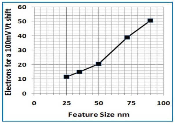
The relentless shrinking of NAND Flash from its inception in 1988 at a transistor gate length of 1000nm to about 1nm in the most advanced form at the time of writing has led to serious challenges that have stalled this progress. An indication of this can be seen in Figure 24 where even single electrons stored on the floating gate have measurable effects on the conductivity of the inherent MOSFET.
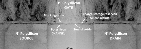
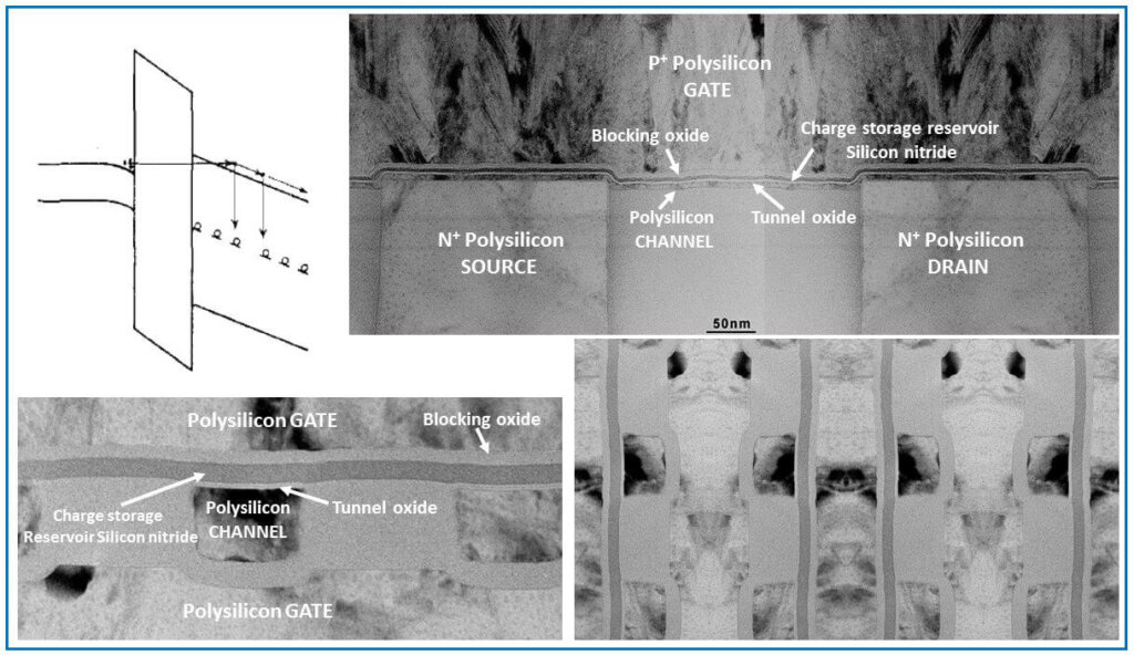
The resultant threshold voltage distributions are unstable due to electron loss and electric field lines resulting from charges not stored in the floating gate. This had led to the invention of various forms of non-volatile memory devices that can be stacked in a 3-dimensional (3D) form to increase storage capacity without having to rely completely on lateral shrinking. Figure 25 shows memory cells in a 3D NAND Flash. Although the approach looks very different from a 2D NAND such as in Figures 22 and 23, the fundamentals are the same: a charge storage reservoir and a field effect transistor.
The structure is a Gate-All-Around thin film transistor with a vertical annulus as a channel. The charge is stored in a silicon nitride layer that is separated from a thin film transistor channel. The channel is made of a deposited layer of polycrystalline silicon. Charge tunnels through a thin tunnel dielectric layer between the channel and the silicon nitride for the program and erase. This tunnel dielectric is made up of layers of silicon dioxide and nitride.
Charge storage affects the conductivity of the transistor channel which can then be sensed in the same way as all the previous MOSFET-based nonvolatile memories.
The cell is much larger than the 2D NAND cell shown in Figures 22 and 23. The total number of electrons stored in the silicon nitride reservoir is therefore much greater resulting in more stability in the threshold voltage.
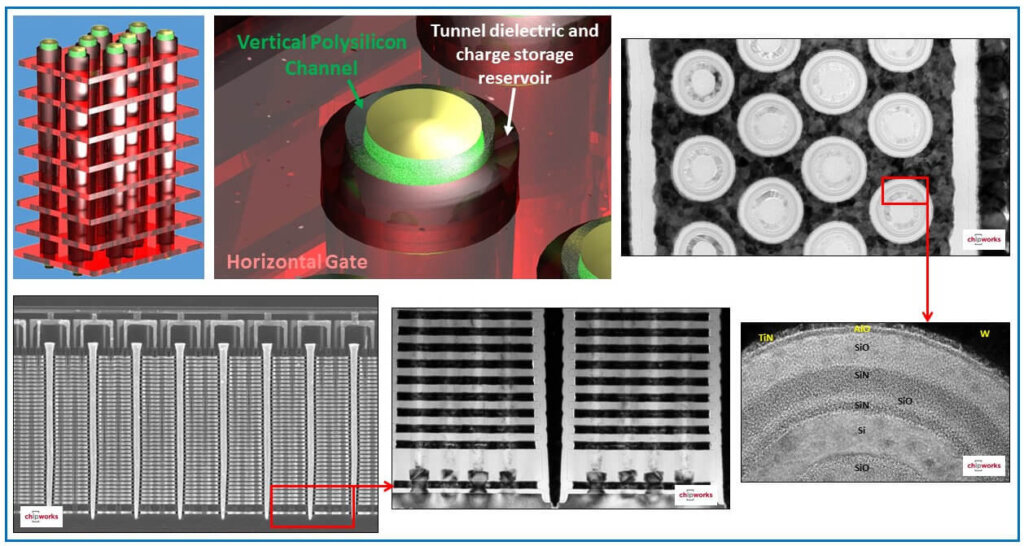
At the time of writing, such 3D NAND chips have been incorporated in the latest products. NAND Flash manufacturers have products with 64 layers and have 96 layers on the horizon. No doubt even taller stacks will come after that.
The two original 1960’s approaches to charge storage are represented in the new 3D NAND Flash, namely silicon nitride as shown in Figure 25, and also floating gate developed by others.
And of course, quantum mechanical tunneling remains as the foundation for the storage of data.
The challenge for the NAND Flash manufacturers is to continue increasing memory densities with a lower cost per memory bit. While great strides have been made over almost 30 years with the last 3 years taken up with conversions to 3-dimensional NAND, challenges have arisen that may impede progress.
One such challenge associated with tunneling is the wear out of the memory cell after program-and-erase cycling. This arises from the fact that Fowler-Nordheim tunneling creates damage in the tunnel dielectric. This can cause unwanted charge trapping and memory retention issues.
As a result, various 3D concepts are being investigated that use a form of quantum mechanical tunneling that had been investigated in the early 1970’s. These rely on direct, not Fowler-Nordheim, tunneling through the tunnel dielectric. This creates far less damage and allows greater program and erase cycling.

Figure 26 shows two of these concepts along with the original energy band diagram from 1973.
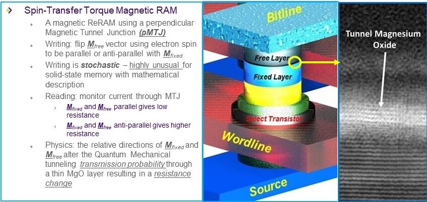
An interesting emerging memory type that depends on tunneling is the Spin-Transfer Torque Magnetic Random Access Memory (STT MRAM). This consists of two magnetic materials, a fixed layer and a free layer, separated by a thin dielectric of magnesium oxide. Quantum mechanical tunneling through this dielectric is modulated by the relative directions of the magnetization vectors of the two magnetic materials, an effect known as tunneling magnetoresistance. The free layer’s magnetization can be changed using the spin of the conducting electrons. This results in a two-terminal memory element with two different resistances. The STT MRAM is emerging as the embedded nonvolatile memory of choice for advanced silicon processes. It is also being touted as a replacement for Static Random Access Memory (SRAM) and, with a small enough memory cell, Dynamic Random Access Memory (DRAM). It is unlikely to replace NAND Flash.
Figure 27 shows the elements of an STT MRAM memory cell with a high-resolution image of the thin magnesium oxide tunneling dielectric.
Quantum mechanical tunneling has formed the foundation for silicon nonvolatile memory storage for almost 50 years. Its incorporation in NAND Flash 30 years ago has driven the digital data storage revolution. New memory cell concepts based on tunneling are being investigated. In addition, many new types of nonvolatile memories are being touted as replacements for NAND Flash. Many of these do not use Quantum Mechanical tunneling.
It remains to be seen how the solid-state storage industry now evolves. Has Quantum Mechanical tunneling had its day or are we on the threshold of further tunneling evolution? ~ A.J.W.
Read the whole series from the beginning.
Acknowledgments
I would like to thank the following people, companies, and institutions for their help in putting together this article. Any errors remaining are all mine.
- Professor Malcolm Longair CBE, FRS, FRSE, Emeritus Jacksonian Professor of Natural Philosophy at the University of Cambridge for reviewing my section on Quantum Mechanics.
- Eli Harari, founder of SanDisk, for great discussions on the early days of Flash cell development and the rise of System Flash and SanDisk.
- Dick James at Chipworks for allowing me to use their beautiful transmission electron micrographs of the most advanced 2- and 3-dimensional NAND Flash cells.
- The Shustek Center at The Computer History Museum for making their archive accessible to me. I had the honor of seeing Martin Lenzlinger’s laboratory notebook when he was at Fairchild.
- Cambridge University Press which was so kind as to allow me to reproduce figures from R.W. Gurney’s Elementary Quantum Mechanics book.