The WeKoPa Resort near Phoenix was the venue for the latest IC packaging focused conference, IMAPS DPC 2017, which took place in early March. The exhibition floor and all the sessions I joined were well attended and covered a broad range of topics, including design tools and methodology demonstrations from both Cadence and Mentor Graphics (as of Friday, 3/31, officially re-branded “Mentor, a Siemens Business”).
I am happy to see that these two large EDA vendors demonstrated their die-package-board design solutions there and showed the IC packaging experts and their customers that packaging is getting (finally) the attention and support it deserves from EDA. These tools enable electronic system architects as well as component designers to reduce risk and development time by simulating which packaging and PCB solution fits their single or multi-die design best and efficiently create system-in-package (SiP) designs for their customers’ application specific requirements.
As usual, on the first day, Monday, March 6, IMAPS offered eight half-day Professional Development Courses (PDCs), focused on modeling, IC design, manufacturing and test topics.
In a morning PDC, I learned from ASE’s Mark Gerber a lot about why and how copper pillars add significant benefits to flip-chips. Here are just a few typical copper pillar interconnect parameters that really drew my attention and should make IC designers evaluate for their next design if/why to use copper pillars (CuP) or wire bonding (WB): 1) Resistance: CuP = 5 vs WB = 50 to 100 milliOhms 2) Inductance: FC = 0.1 vs WB = 1 to 4 NH 3) Length: FC = 3 to 6 vs WB = 50 to 100 mils.
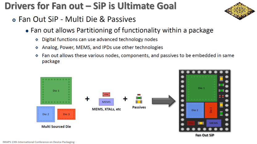
In his afternoon PDC, ASE’s John Hunt gave an impressive tour through the rapidly growing fan-out wafer level packaging (FOWLP) technologies. Here are a few key points I captured: FOWLP allows even lower package heights then CuP flip-chips, tighter spacing and of course offers all other benefits of wafer-level processing – or panel-level in the future.
While different vendors offer a wide range of FOWLP alternatives (Focus, SWIFT, SLIM, SLIT, …) the currently most widely used technology is Infineon’s embedded wafer-level BGA (eWLB), also available from ASE.
To maintain good yields, while package geometries continue to shrink and manufacturing tolerances are getting tighter, ASE has licensed Deca Technologies’ adaptive patterning and routing technology for both single and multi-die assembly.
Hunt also gave several examples of FOWLP technology supporting heterogeneous integration, a key stepping stone towards entire SiPs (Figure 1). Last, but not least, Hunt mentioned that customers start asking about alternate sourcing for these advanced packages. A clear sign that volumes increase significantly and more of designs’ value creation and differentiation is moving from the die to the package.
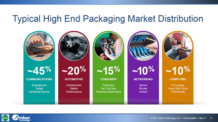
Tuesday morning the regular conference started with two keynotes. Amkor’s Ron Huemoeller delivered the first one. Within the first few slides, Huemoeller demonstrated that there is no ”one size fits all” thinking in IC packaging and explained why our industry’s major market segments have very different requirements for assembly and test houses (Figure 2). He also talked about how the current mergers and acquisitions wave is driving consolidation of outsourced semiconductor assembly and test companies (OSATs).
Amkor and ASE, the two largest OSATs, share now 45% of the market because advanced IC packaging is getting much more capital intensive – similar to manufacturing wafer – and puts smaller companies at a disadvantage. In addition, the many different package types and customer requirements force smaller OSATs to focus on very specific segments and technologies to remain competitive.
Lionel Rudant, Strategic Marketing Manager at Leti, outlined in his keynote why and how ubiquitous communication, enabled by 5G wireless technology, will change the world around us. He showed a number of examples how 5G will change, e.g. traffic in cities. Rudant projected that 5G will be selectively deployed at the Olympics in Korea in 2018, then broadly rolled out in 2019/20. Another key point I captured: 5G carrier frequencies are about 60 GHz, which means they use mm-waves and make antennas small enough to fit into IC packages — another big benefit SiP technology offers to make mobile devices smaller and smarter.

Let’s address the many informative conference presentations between the two “keynote session bookends” in part two of this IMAPS blog (to be published shortly) and jump to the last two keynotes given on Thursday morning, the final day of the conference:
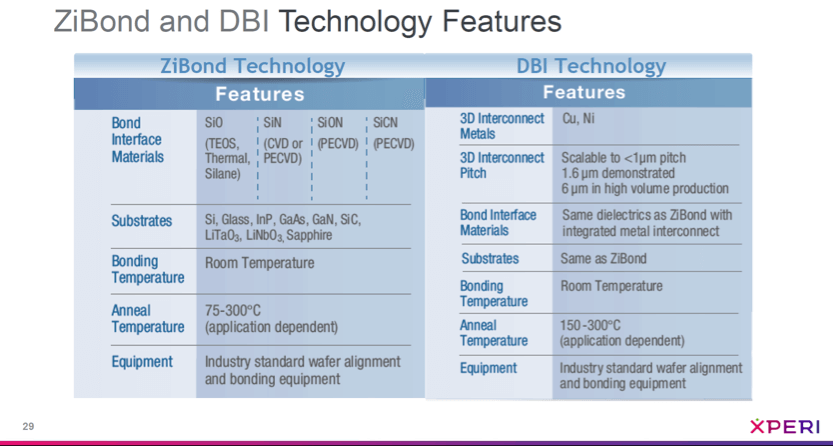
Sitaram Arkalgud drives utilization of ZiBond® and DBI® 3D interconnect technologies at Invensas, a subsidiary of Xperi. He outlined how ZiBond, their low-temperature oxide to oxide bonding technology is used for wafers bonding and how DBI, a very fine-pitch copper to copper interconnect technology, is used in applications that require many and very high-density vertical connections, e.g. SONY’s high-resolution image sensors. Another example for designs requiring a large number of vertical connections, that’s benefiting from DBI is Tezzaron’s family of memory cubes.
Arkalgud also introduced the new Xperi and its subsidiaries – DTS / FotoNation / Invensas / Tessera – and how these corporations’ focus on rapidly emerging markets. As more of our electronic devices need to communicate with the world around us, MEMS and sensors are needed to make them get all or at least some of the human senses. These MEMS and sensors need to be reliably and cost-effectively interconnected with logic, memory, analog, RF,… functions in these smart devices. Arkalgud summarized in Figure 3 below the features and benefits of Xperi’s bonding technologies.
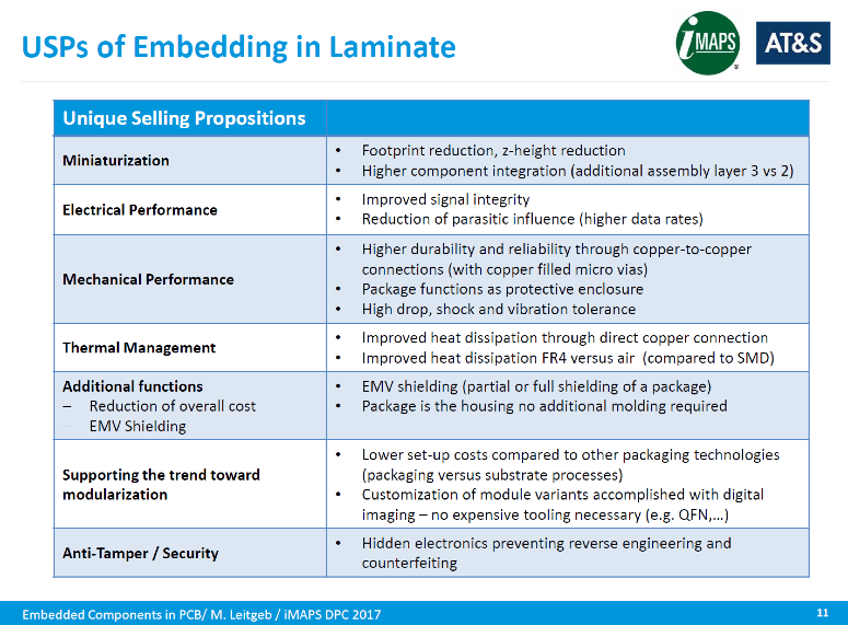
My Austrian countryman, Markus Leitgeb from AT & S, delivered the fourth keynote. After introducing “Austria Technology & Systemtechnik” (AT&S) he introduced their high-end PCB capabilities, described their benefits for mobile devices, medical/industrial/automotive and other applications and showed a long list of high-tech companies using AT&S products. Leitgeb also outlined the embedded die technology AT&S developed and explained how and why designers utilize it. He outlined a number of reference designs for both their PCB and embedded die technologies, showed how well AT&S is integrated into Consortia and listed Altium, Mentor, Cadence and Zuken as their EDA partners.
Let’s close by looping back to the EDA contributions at this conference more:
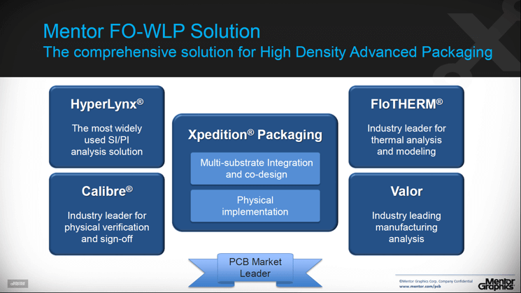
Cadence demonstrated and explained on the exhibition floor their design flow for TSMC’s InFO packaging. Mentor explained during the poster session the reference flow they developed and announced together with TSMC. The summary slide below shows all the tools deployed in Mentor’s FOWLP design solution.
Looking forward to your feedback to this, part 1, and to part 2, of my IMAPS Phoenix blog, which is coming soon. Regards….Herb