


Every year, I attend most of the events that are focused on 3D integration and related approaches to semiconductor advanced packaging. One thing that I’ve heard over the past year is that as 3D technologies move into manufacturing, it’s become difficult to recruit speakers who have fresh content. Notoriously slow to evolve, the 3D integration conversation hasn’t changed too much over the past year. Now that it’s happening, customers have become hush-hush about what they are doing. As such, we’re treated to a lot of recaps and retrospectives, which is great for newcomers to the market, and not so great for veterans like me. That said, I must commend the committee who pulled together the 2017 European 3D Summit and found a way to mix it up a bit by inviting new speakers from different segments of the market, and addressing the topic: Achieving High-density 3D Systems.
I was asked to deliver the closing remarks on Wednesday, and afterward, a few people asked when I would be publishing those remarks. What follows is a slightly expanded version.
As I’ve attended this event since it began five years ago, I want to reflect a moment on what has changed. The definition of 3D has evolved. It used to be that if through silicon vias (TSVs) weren’t involved, we weren’t supposed to call it a 3D technology, so said the purists. Now everything that takes the package into the Z-direction, from wire bonded stacks, to package-on-package, to 3D fan-out-wafer-level-packages (FOWLP), embedded die and 3D IC is fair game. The content itself also represented a shift in focus, with recently hot topics down to one presentation each (materials – Dow Electronic Materials; glass substrates – Samtec Microelectronics; and processes for FOWLP – Evatec), and added emphasis on design, simulation, and modeling for high-density systems and thermal management.
Juergen Wolf, Fraunhofer IZM-ASSD told us that 3D packaging is driven not by technology, but by applications. As an example, the Apple watch contains 13 wafer level packages (WLP) and one system in package (SiP). He also noted that 80% of automotive innovations come from electronic devices, and proved it by showing us a cool video of a BMW concept car that is both driver-assist and autonomous. Wolf cited options for reducing TSV cost, such as via first vs. via last, smaller TSV diameter, processes for barrier/seed depositions, wafer thinning, and skipping bumps and forming direct interconnects instead.
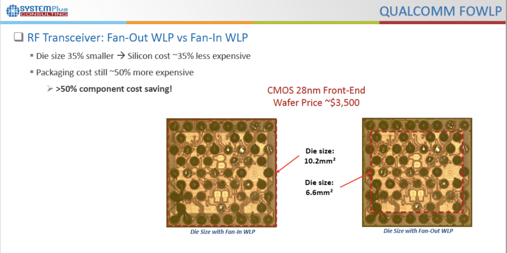
Using teardown reports of various packaging types, Romain Fraux, System Plus provided an updated technical and cost review of 3D packages. In his comparison of fan-in vs. fan-out wafer level packaging (FOLWP), the results varied based on the node and application. While it seemed that fan-in was the winner at 40nm with a .07 cost per component vs. .10 for FOWLP, he did note that for RF applications, FOWLP represents a 50% overall component cost savings over fan-in (Fig 1). In a comparison of a variety of 3D FOWLP-PoP packages from Amkor, TSMC, and Shinko (used in Qualcomm’s snapdragon, InFo offers a 30% reduction in package thickness because flip chip steps are removed, and there is no laminate substrate.
Thibault Buisson, Yole Développement, noted that our smartphones will have 20 sensors by 2021, which calls for WLP and 3D packaging. Many segments and applications are driving the markets, including IoT, wearables, AR/VR headsets, and automotive, as well as high data centers, and deep learning.
David Butler, SPTS, presenting on behalf of Jan Vardaman, TechSearch International, said that TSVs are finally in our smartphones in image sensors and fingerprint sensors, but still not in DRAM on logic. TechSearch’s forecast predicts that by 2018, we have the potential to reach close to .5 million wafers, which by comparison isn’t a lot, but what we don’t have in volume, we’ll make up for in high dollar values.
Mustafa Badaroglu, Qualcomm, talked about 3D VLSI system-on-chip (SoC), which uses a sequential process to create “true” 3D IC stacks for high density interconnects. He said the need for 3D VLSI SoCs is driven by edge and cloud computing. Edge computing refers to the need for instant data generated by sensors and the user. By comparison, big data and abundant computing power are pushing computing to the cloud. Hybrid bonding is a critical component to 3D VLSI SoC.
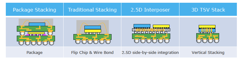
For those new to 3DICs and 3D packaging (there were a number of newcomers in the audience) Thorsten Meyer, Infineon explained the different ways to build 3D stacks (Figure 2). He broke down the difference between package and traditional stacking, 2.5D interposer, and 3D TSV stacks, and then talked about Infineon’s approach to using embedded die technologies to achieve next-generation interconnect density requirements.
Silicon photonics was discussed during several presentations. For example, Jihan Chen, ASE, explained how Si Photonics in SiP packages enables optical engines that solve Ethernet switch challenges. He showed a multi-chip integration approach to integrating electronics and photonics into one package using FO SiP. The advantage is a short RDL path for high-speed signals.

On the topic of Moore’s law scaling vs. 3D ICs, Xin Wu at Xilinx noted that 3D IC doubles capability of FPGA at future nodes. He pointed out that mature technologies still provide the best cost benefit. It’s not about a good solution or bad solution, just one that is more or less suitable. He also said that customers don’t adopt new tech for 10% cost savings, but will for a performance boost.
As noted during the 3D ASIP conference, wafer-to-wafer hybrid bonding is the magic solution to everything from lowering cost, to enabling sequential stacking, to reducing thermal resistance. At both conferences, direct bond interconnect (DBI™), Invensas’ trademarked name, was used interchangeably with hybrid bonding, which begs the question, is there more than one kind of hybrid bonding out there? And if you’re considering using hybrid bonding in your processes, should you be licensing the technology from Invensas? My opinion? Better to err on the side of caution and check it out.
Plasma dicing seems to be a hot new topic, taking on the traditional saw dicing approach. Both Reinhard Windemuth, Panasonic and David Butler, SPTS presented their companies’ plasma dicing offerings, and both talked about the advantages of this vibration-free process, which can dice thinner and smaller die in any shape, without needing water. Plasma dicing is damage-free, resulting in better yield. Both Panasonic and SPTS offer similar solutions, including end-point detection, which is an important feature to have, noted Butler.
From the research community, we learned about a number of efforts being made to understand the thermal management issues of interposer and 3D packages, and learned about possible solutions including microfluidics cooling channels, from Luc Frechétte, University of Sherbrooke, as well as a thermally aware design that combines liquid cooling plus power generation, from Marina Sapater, EPFL.
Applied Materials’ Sesh Ramaswami addressed the topic of panel level packaging, and whether or not we will see it realized. He said some learning from wafer level processing can be translated to panel process, but a materials, equipment and integration inflection point needs to be reached. While good work has occurred in academia to establish learning, industrial challenges for panel level processing could be significant.
According to Wenqi Zhang, Director R&D, NCAP, China holds the #2 position globally for packaging. NCAP is fostering Intensive collaboration with local equipment and material suppliers. Currently, China is two generations behind on technology, noted Zhang, but 3D high-density technologies offer them the opportunity to increase capabilities. As such, NCAP fostering collaborative innovation through a national project focused on 3D high-density systems.
In summary, the 3D story hasn’t changed much since last year. As predicted, TSVs started in HPC applications, image sensors, MEMS and memory, and will be adopted as performance call for it and as the cost comes down. Smartphones are still a key driver, even as industrial applications grow. While overall semiconductor growth will be about 4%, the highest growth is expected to be in the advanced packaging sector.
As the industry refocuses on heterogeneous integration, there is a new appreciation for advanced packaging technologies as a value-add vs. a cost adder. 2017 should be interesting, and we can expect next year’s 3D Summit, scheduled for January 22-24, 2018, to be an exciting one as we make advanced packaging great again. ~ F.v.T


