


Part three of a five-part series
 In the first two parts of this series, we focused on low-cost flip chip and wafer-level chip scale packages (WLCSP), identifying them as two advanced packaging platforms we consider to be among the “Big Five.” It is our belief at Amkor that convergence into these five platforms is driven by the shift away from PCs and notebooks, toward mobile devices, wearables, and the Internet of Things (IoT). The remaining three platforms include advanced MEMS, laminate-based advanced system-in-package (SiP) and wafer-based advanced SiP. This installment focuses on advanced MEMS packaging.
Many predict that the growing trend for smart devices, cars, cities, industry, etc., calls for the development of a trillion sensors, many of which are micro-electromechanical systems (MEMS). Why so many? Because everything that needs to be smart begins with a sensing device and some end with an actuating device. Further, consumers want their devices to anticipate their needs. For example, we want our phones to intuitively tell us when our next appointment is, who it’s with, where it is, how long it will take us to get there based on traffic conditions, and what time we need to leave to be there on time. This requires the phones to gather this information from sensors in the phone, as well as along the route and turn it into actionable data.
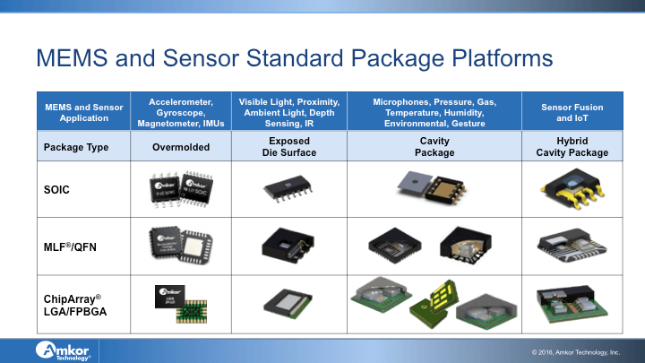
MEMS and Sensors Packaging
MEMS devices are not standard integrated circuits. Creative wafer fabrication techniques produce Si-based transducers and actuators that respond to or interact with, external or environmental stimulus. At the onset of MEMS packaging, priority was given to solving the end-market application over cost and package form factor. This created a broad diversity of package form factors, with a different approach for almost every application and end market. As the MEMS market grows and transitions into high-volume production, the drive toward package and test standardization is needed to offer cost-competitive solutions without sacrificing performance. The requirement to control stress to the MEMS structure while allowing stimulus to go through remains the same. The combination of a standard cavity packaging platform and optimized material sets will ensure a near-stress-free environment that allows the MEMS to function as it was designed to in the real world.
Amkor’s focus is creating a standard cavity package platform that will provide the flexibility to support multiple MEMS applications. It will be customizable on the inside while remaining standard on the outside to maintain maximum compatibility during assembly, final test, and surface board mount. The standard MEMS platforms will also allow Amkor to use other packaging technologies like FlipStack®, through silicon via, Cu pillar, and die stacking for MEMS sensor fusion and IoT applications.

Conclusion
Sensor fusion leverages all of our advanced packaging expertise to integrate different MEMS and sensor functionalities to create multi-die packages. FlipStack technology is an example of sensor fusion, in which the bottom ASIC die is a flip chip, and then the MEMS die is stacked on top and wire-bonded to reduce the overall package footprint.
At Amkor, we believe our advanced MEMS packaging platform and the rest of the Big Five sets us apart from our competitors, as we strive to deliver reliable options that suit client needs at optimum cost and performance. ~ A. Arcedera
The fourth installment in this series on “The Big Five” focuses on laminate-based advances SiP.


