
Part two of a five-part series.
 How did we determine which technologies are “the Big Five,” for semiconductor packaging? Essentially, we identified the five key platforms that we believe will be leveraged across a multitude of applications and markets now and in the future. The selected platforms are low-cost flip chip, wafer-level chip scale packaging (WLCSP), micro-electromechanical systems (MEMS), laminate-based advanced system-in-package (SiP) and wafer-based advanced SiP. These key packaging technologies are currently in different stages of adoption and production, and will hold up through generations of development to continue serving the industry needs. With these five platforms in our arsenal, we will be able to provide the lowest-cost solution to meet the reliability needs of the customer, regardless of the package type and structure.
In Part One of this series about the convergence of advanced packaging to the Big Five, we focused on low-cost flip chip, which is an enabling interconnect technology. In this segment, we will focus on WLCSPs.
What Is WLCSP?
A WLCSP is an advanced packaging technology that does not have a package substrate and is mounted directly onto the printed circuit board after being bumped. It is a single-die package that is limited by the die size. More descriptively, it includes wafer bumping (with or without pad layer redistribution), wafer-level final test, device singulation, and packing in tape and reel to support a full turnkey solution.
Now in volume production, WLCSP is the workhorse of the Big Five advanced packaging technologies due to its cost/performance ratio resulting from the elimination of the package substrate. Packaging considerations start with WLCSP, and only move to other formats when routing requirements exhaust the available real estate. Ultimately, customers will choose WLCSP over the other package options where technologically possible because it’s the lowest-cost package.
Applications and Markets
Also known as fan-in wafer-level packaging (FI-WLP) industry-wide, Amkor’s WLCSPs are applicable to a wide range of markets; are generally related to analog and mixed-signal, wireless connectivity, and automotive device categories; and include applications like integrated passive devices, codec, power amplifiers, IC drivers, RF transceivers, wireless local area network chips, GPS, and automotive radar. WLCSP offers the lowest total cost of ownership, enabling higher semiconductor content while leveraging the smallest form factor. It is one of the highest-performing, most reliable semiconductor package platforms on the market today. From a market perspective, WLCSP is ideally suited for, but not limited to, mobile phones, tablets, netbook PCs, disk drives, digital still and video cameras, navigation devices, game controllers, other portable/remote products, and some automotive end applications.
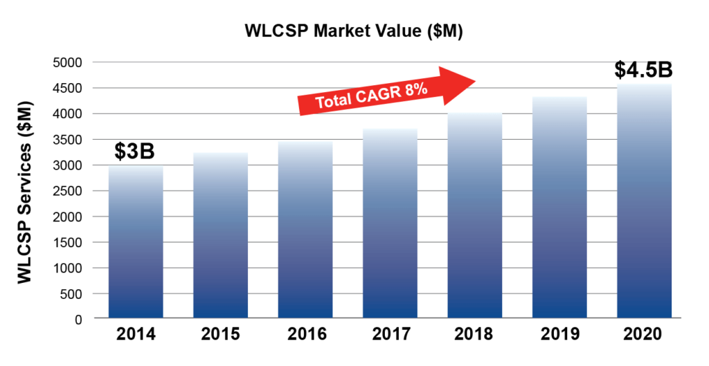
Historically, the WLCSP has been driven by the handset, tablet, and computing markets; and more recently, the automotive and wearables market. Today, 30% of the packages in high-end smartphones are WLCSP. According to Yole Développement, the WLCSP market is expected to grow to $4.5B by 2020 from $3B in 2014, representing an 8% CAGR (Figure 1). This market estimate includes wafer-level, die-level, and test services. Additionally, WLCSP manufacturing continues to be dominated by outsourced semiconductor assembly and test service (OSAT) providers. According to Yole, out of the top 10 manufacturers, eight are OSATs; one is an integrated device manufacturer (Texas Instruments); and one is a foundry (TSMC).
Perpetual Innovation

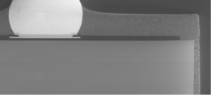
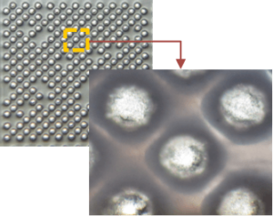
Perpetual innovation is intrinsic to packaging success and focuses on driving existing technologies to lower cost points. With the anticipated growth in the WLCSP market, there are many reasons for improving and optimizing the WLCSP manufacturing process. A good example of optimization is the implementation of die sidewall protection. Although most WLCSPs are not molded, Amkor has developed a method of providing mold-like die surface protection. Using this approach, Amkor injects molding into the saw streets, and then the wafer is diced again, creating five- and six-sided molded WLCSPs (Figures 2a and b). This process is currently available, and customers are now designing this into their WLCSP requirements.
This protection becomes even more critical as silicon nodes scale beyond 14nm to 10nm and 5nm, where the risk of potential sidewall damage intensifies due to brittle dielectrics, smaller bump pitches, and more.
At Amkor, we are committed to the continued improvement of key packaging platforms like WLCSP, together with the development of more advanced platforms that include laminate SiP and wafer-based SiP.
The third installment in this series on “The Big Five” focuses on MEMS and sensor packaging.