


It is often claimed that 3D chip stacks offer the potential to meet current and future requirements of digital circuits, such as for performance, functionality, and power consumption. Specifically, both design paradigms “More Moore” and “More than Moore” will benefit from 3D chip stacking (and new technologies and materials).
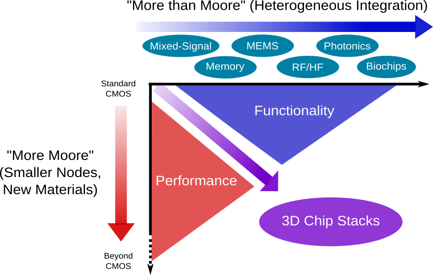
3D stacking enables notably reduced interconnect lengths and, thus, reduced delays and increased performance. At the same time, heterogeneous components designed using different technologies across multiple dies are relatively easy integrated into one common stack. Note that heterogeneous stacks, if tailored for small footprints and low power consumption, are also essential for widely-anticipated applications such as the Internet of Things (IoT).
Despite significant projected benefits over 2D chips and the recent emergence of 3D memory stacks (such as High-Bandwidth Memory, HBM), the overall adoption of 3D stacks still lags behind expectations. What are reasons for the current lack of adoption, and what are specific implications for physical design automation?
Successful adoption of 3D chip stacks requires addressing different classical and novel challenges which simultaneously affect the manufacturing processes, design practices, and physical design tools. If not properly addressed, these fairly complex challenges (such as adverse multi-domain coupling effects) may render 3D chip stacks commercially unviable, despite recent advances in manufacturing yield and cost reduction. Physical design automation partially meets these challenges at present, but further efforts are needed to fully exploit the potential of 3D chip stacks and to facilitate their commercial breakthrough.
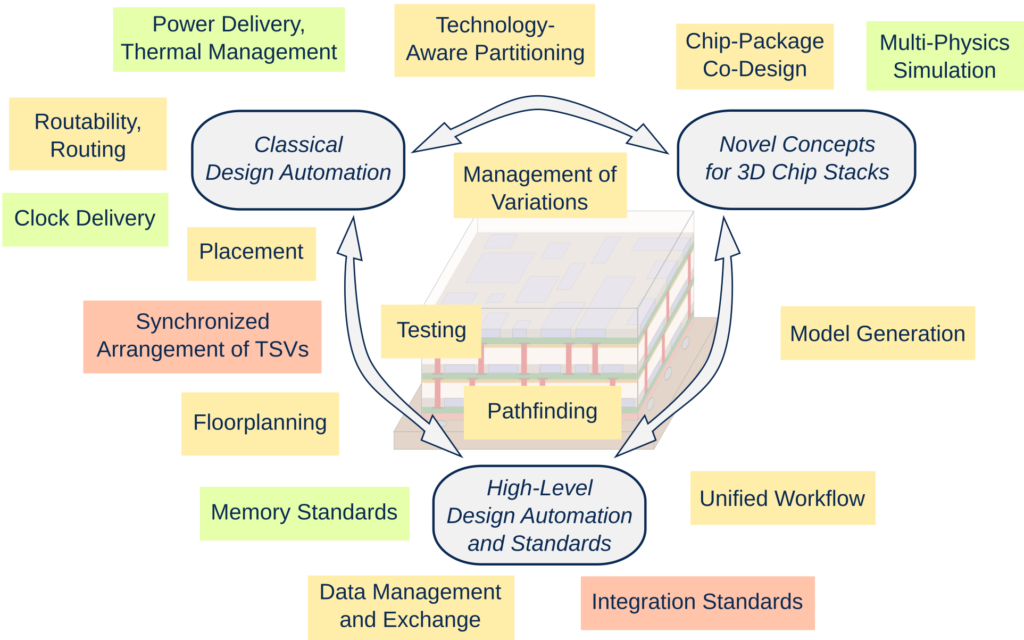
In our open-access tutorial paper, we first review the diversity of stacking options for 3D chips and formulate related high-level design challenges. Then, we discuss the following classical challenges and related promising electronic design automation (EDA) solutions:
- Power delivery and thermal management;
- Clock delivery;
- Partitioning and floorplanning;
- Placement;
- Routability estimation and routing; and
- Testing.
We highlight how these challenges have become increasingly difficult and demanding as compared to well-engineered design automation for 2D chips, and we review the state-of-art for such 3D-chip design automation.
We also elaborate on novel challenges that are currently (at least partially) addressed, such as:
- Pathfinding and high-level design-space exploration;
- System-level design of interconnects;
- Unified workflow;
- Chip-package co-design; and
- Multi-physics simulation and verification.
One such novel challenge is the need for a unified workflow. Given the plethora of already available (2D) tools, novel/upcoming (3D) tools and various design practices and design know-how, all distributed among multiple design parties, the introduction of a common workflow is essential. Within a unified workflow, different design tools/stages are interacting across different levels of design hierarchy: pathfinding and prototyping are interleaving with both high-level/chip-package design and detailed design.
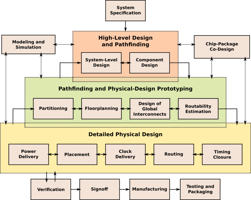

Thus, pathfinding and prototyping link system-level and IC-level design, easing design closure for the highly iterative 3D-design process. Note that the concept of a unified workflow calls for extensive use of internal/external APIs and for file formats tailored for exchanging 3D design and simulation data.
Overall, we conclude that design automation for 3D chip stacks is complex and not all challenges are fully solved yet, though more and more sophisticated EDA solutions are being proposed.
The multitude of these challenges is one major contributing factor to the problem mentioned at the beginning, which is the slow commercial adoption of 3D stacking. But with many of the classical challenges for physical design solved already now or to be solved soon, we can expect 3D chip stacks to become available not just for memory applications, but also for logic integration and IoT devices. Recent efforts such as assembly design kits (ADKs) and pathfinding tools, among others, help to streamline this adoption process further.
This tutorial was presented in detail on April 4, 2016, at the 25th International Symposium on Physical Design and on October 2, 2016, at the 34th IEEE International Conference on Computer Design.
Download our open-access paper for more details, and get the for ICCD 2016 extended and updated slides.
Figures courtesy of J. Knechtel, J. Lienig “Physical Design Automation for 3D Chip Stacks – Challenges and Solutions,” Proc. of the ACM 2016 Int. Symposium on Physical Design (ISPD’16), Santa Rosa, CA, pp. 3-10, April 2016.


