


Last June, AMD made 3D integration history with its introduction of the Fiji gaming processor unit (GPU), which for the first time put high bandwidth memory (HBM) — a true 3D stack integrating memory die with through silicon via (TSVs) — into production. Fiji is a Si interposer-based module comprising an ASIC GPU surrounded by 4 HBM stacks, and it is powering AMD’s latest generation of Radeon Fury graphics cards for high-performance gaming. This event was a turning point for HBM, putting it ahead of Micron’s much-hyped Hybrid Memory Cube (HMC) as the go-to memory for high performance computing and networking applications. Since then, a number of companies have ramped their HBM programs into high gear and developed an HBM supply chain.
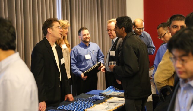
I was invited to emcee a seminar entitled, “Start your HBM/2.5D Design Today”, which took place on March 9 at the Computer History Museum in Mountain View, CA. It was a fitting venue for this event, as it represents the work of so many of the industry’s pioneers. The seminar featured presenters from five unique companies who have successfully developed an interposer-based HBM supply chain that has all the parts in place to ramp to volume production.
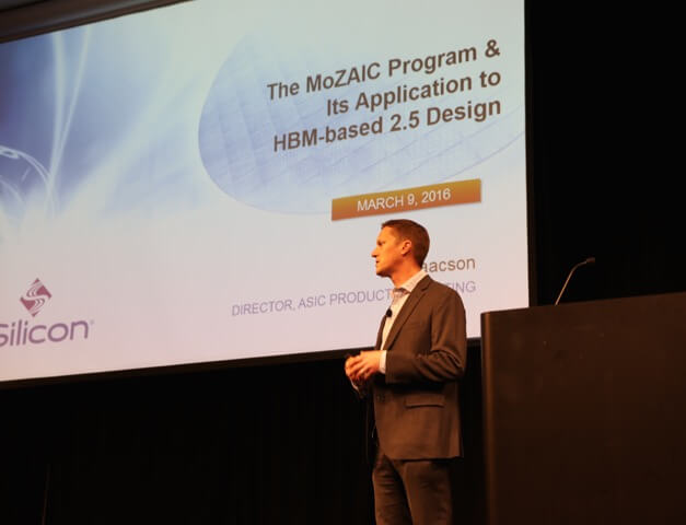
Kevin Tran, SK hynix; Paul Silvestri; Amkor Technologies; Bill Isaacson, eSilicon; Brian Daellenbach, Northwest Logic; and Chris Browy, Avery Design each described his company’s capabilities, and the role it plays in this supply chain. SK hynix provides the HBM stack. eSilicon is the ASIC vendor and system integrator. They work with the system architect to engineer the ASIC, and also design the interposer and package to deliver a turnkey solution. eSilicon also provides the HBM PHY and will own the yield for the final device. Northwest Logic provides the controller IP for the ASIC, Avery Designs provides the verification IP; specifically an HBM model used to verify the system. Amkor does the heavy lifting; integrating the HBM, interposer and ASIC wafers into a 2.5D assembly, and testing and shipping the module to the end customer. The message for the day: the HBM supply chain is open for business.
While I won’t dive into all the details of the presentations, here are some of the key take-aways:
- Silvestri noted that TSVs should no longer be considered an R&D technology, but should be considered a production ready product. He noted that incoming interposer wafers from various sources demonstrate consistently good quality.
- In response to the cost comparison of HBM vs. traditional DRAM, Silvestri said it’s difficult to cost-compare a package with basic memory vs. one with HBM. For example, in the case of the Fiji processor, they took memory traditionally placed “outboard” with wire-bond interconnects, vs. taking all the memory and stacking it on the interposer. Yes HBM adds cost to the package, but it’s the system-level cost needs to be considered.
- Isaacson explained that cost analysis has shown that the HBM-based solution to increased bandwidth is considerably less expensive at system level, just in terms of ASIC real estate. To get the 2Tb/second of bandwidth that you get with a single HBM (12sq. mm) requires roughly 40 DDR4s (300sq mm). “If your object is increased bandwidth, than you win with HBM,” he said.
This fact is becoming very apparent to system architects. Browy told me that in the past six months, the demand for HBM solution has “exploded.” Three years ago, noted Daellenbach, the hybrid memory cube (HMC) had the market lead on HBM as the memory solution for high performance computing and networking, and was expected to be the winner. But HBM has leapt ahead for a number of reasons: There are a number of sources because it’s a JEDEC standard. It’s also a lower power, and a lower cost solution than HMC. Reportedly, there have also been thermal issues with HMC due to the SERDES.

So how does this particular collaborative supply chain work? “HBM is the starting point, because they are looking for a solution to the bandwidth problem, and the ASIC isn’t the problem; it’s the memory that’s the problem,” said Tran. He said SK Hynix established the ecosystem along with eSilicon and invited the other companies to join in, because HBM is so complicated to adopt. “Unless we set up a supply chain with solutions that are ready, OEMs won’t be willing to invest,” he explained. While all the supply chain members recognize one another as the preferred vendor for their roles, it is an open supply chain, and customers are welcome to work with any or all of the companies. However, the benefit of working with the full supply chain is that they have invested in the R&D and have experience working with using this technology. According to Isaacson, they have built several test vehicles starting in 2011. He also showed two production designs for HPC and networking, one at 28nm and one at 14nm, that will ramp to volume this year.
If you missed the seminar, the group is hosting a webinar on March 29, 2016. It will be scheduled for two different times to accommodate time zones. Additionally. they will be publishing a white paper, which will be delivered to those who attended the seminar and register for the webinars. Look out for details coming soon.


