The Computer History Museum in Mountain View is a very impressive place to show you the enormous progress ICs and Electronic Systems have made in the most recent 50+ years. What I like even more is the fact that an increasing number of high-tech companies and industry organizations are utilizing this great facility for charting our future path on the innovation curve with exhibitions, seminars, workshops and social events.
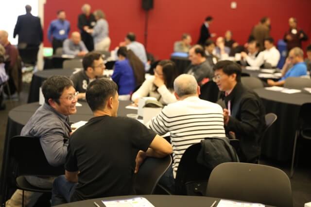
Last Wednesday, March 9, five very important drivers of interposer-based (a.k.a. 2.5D) ICs presented their products and services and demonstrated that they make it easy for system- and IC designers to utilize the many benefits this technology offers. SK Hynix outlined their impressive HBM (high bandwidth memory) cubes, Amkor showed their breadth of advanced packaging technologies, eSilicon highlighted their experience with architecting and implementing customer designs in 2.5D-ICs (so far 7 designs done), NorthWest Logic outlined their HBM controller building blocks and Avery Design Systems showed their breath of verification IP, including HBM support.
Fairly brief, concise and very compelling presentations set the stage for every one of these five topics. Plenty of time for Q&A assured that the audience got their specific questions addressed and lingering concerns eliminated. I found bringing key players for interposer designs into one room, to be very strategic and helpful. This event offered the five companies not only time for presentations, but also room for tabletop exhibits and plenty of opportunities for in-depth customer interaction. I’ll take the liberty and copy some of the organizers ideas – hopefully royalty-free – at the next such events I’ll organize.
After more than eight years of, initially blindly, more recently much more targeted business development work for multi-die integration and advanced IC packaging, allow me to share a few suggestions for further improving such events in future.
Try to get system architects and C-level engineering executives to also attend and challenge them to join the discussions.
During the many presentations I gave as “2.5/3D-IC missionary”, these experts asked the best questions, translated the new technology features right away into specific and very tangible system-level advantages (e.g. great performance per Watt, space & weight savings, lower SYSTEM cost, shorter development time,…) and motivated the IC designers to look at the system-level context too.
Invite a SYSTEM cost model expert to present as well. The initial component cost is always higher than the cost of mature components. This, initially steep cost differential, makes project managers and IC designers hesitant to plan using the new technology – even if it’s on a steep cost-reduction curve, like advanced multi-die packaging is today.

Getting C-level executives to pay attention to a new technology, like 2.5D-ICs, which most likely will initially only get deployed in a less important and low revenue application, is of course very difficult, but it’s really necessary now. I am glad that magazines targeting high-level executives are covering the challenges our industry faces, with the end of Moore’s Law. From a technical perspective and for ultra-high volume designs, there may be a few nodes left. However, from a commercial point of view, most applications are already no longer able to pay back the enormous development cost of sub 14/16 nm designs. We need to act NOW.
Let’s close on a very positive note and show you that we are not alone in our efforts to change the IC integration paradigm. Here are web-pointers to an excellent article in Forbes Magazine, a brief Economist article about the future of computing and to the most recent Technology Quarterly in this week’s edition of the Economist. Both Economist and Forbes are favorite reading materials for our industry’s decision makers and will help our “multi-die and advanced packaging” cause with these referenced articles.
There is no need to worry about our industry’s growth potential, as long as we move on, together, from transistor scaling to SYSTEM scaling and utilize the rapidly emerging advanced IC packaging technologies for multi-die integration.
~ Herb