


During the 2015 European 3D TSV Summit, I drove attendees to distraction by asking each presenter what success looked like to them for 3D integration. The resulting responses became a blog post, What Does Success for 3D Integration Look Like? Now, a year later, I decided to revisit the topic by reminding last year’s presenters of their responses, and asking them for an update. As only few of the 2015 presenters presented at the 2015 European 3D Summit, I had to track down some of the responders. Some report great success, some moderate, and some have shifted focus of success to include fan-out wafer level packaging (FOWLP). Ampmg those I spoke with, here’s what they had to say:
- Last year, Jan Vardaman, TechSearch International Inc, said:“Success is when I can go into a store and buy a product to tear down and find a 3D IC inside.” This year’s response: “Since AMD is shipping a product that has both a 3D IC with TSV stack and a silicon interposer, I would say the industry is successful in the commercialization of this technology. Cost and other factors limit some of the applications to high-performance, which makes unit volumes smaller. Sony is seeing success with its camera module using stacked image sensor and logic in mobile applications, but we will not see a memory and logic (application processor) stack in the mobile phone because of cost, business issues, thermal issues, and the fact that FOWLP offers almost the electrical performance benefit that could be provided by a memory and logic stack with TSVs.
- In 2015, Rozalia Beica, Yole Développement defined success as entering volume production, and that overcoming the challenges so far was a step towards final success. So have we been successful? “I think so, yes,” she said. “We still have a ways to go to high volume production, but it seems end customers are seeing the advantages, and more and more products with 3D technologies are going into production.”
- While Scott Jones, Alix Partners, didn’t present this year, last year he said “When I can go buy an iPad and it has 3D inside; when Intel and Samsung stands up here and says we have it, that’s what we see as success for this technology.” While no one from Intel or Samsung presented at this year’s summit, Samsung has gone into volume production with two memory stacks using 3D TSV technologies: their 3D TSV DDR4 and most recently, HBM2 DRAM. Additionally, Intel announced they will be implementing 2.5D and 3D technologies in 2016. Sounds like success to me.
- For Eric Beyne, imec, last year, the most important thing for success would be adoption in to the market. As 2015 brought a number of 3D stacked memory products to the market, Beyne says, “We were right. It’s happened 100%.” So what’s next? “higher density wafer bonding is a bit further out in applications, but it’s coming.”
- Last year, Farhang Yazdani, CEO Broadpak said success would be achieving a low cost secure system that is easy to integrate and is cost effective. So have we achieved this level of success? “I think we are there,” he said. “The price of silicon interposers has substantially been reduced, this is evident in the number of requests we have received.”
- Georg Kimmich, ST Microelectronics, said last year that success for 3D was more about performance than cost, and was already successfully being implemented in image sensors. The next measure of success would be photonics. This year, he was happy to report that ST Microelectronics have built a photonics prototype, “so we’re getting there.” He added that in his opinion, FOWLP is all hype just because Apple and TSMC are doing it. “It’s (FOWLP) only a replacement for PoP in smartphones and IoT applications, where the main concern is cost.,” he said.
- Also on the topic of photonics development, Marco Fiorentino, HP Labs, defined success as a device that includes both the photonics and the TSV available from a foundry. He reported that they are not quite there yet, but hopes that work will continue in the coming year.
- Last year David Butler, SPTS, said success would be when the OSATS are working in a similar direction, and not working on three or four technology types. Have we made progress? “I think we’re getting into that phase now, but perhaps not in the way we envisaged a couple of years ago. In 2016, the focus on TSV has softened, to be replaced by FOWLP with all OSATS and a number of foundries working hard to be ready for a fast ramp. Unlike TSV technology where the underlying concern was will it ever get into HVM, FOWLP will go into significant volume in the 2nd half 2016 and continue on a fast growth right through 2020. It does feel like a technology whose time has come, both in terms of costs and of density. “
- Martin Schrems, AMS, had said last year that if the forecasts held or exceeded predictions for use of 3D integration and wafer-level packaging, he will consider that success. The verdict? “In our case, its taken a longer time coming than many people thought,” he said. “The good news is, its coming now. Success is really around the corner. If you look closely. Its already happening.”
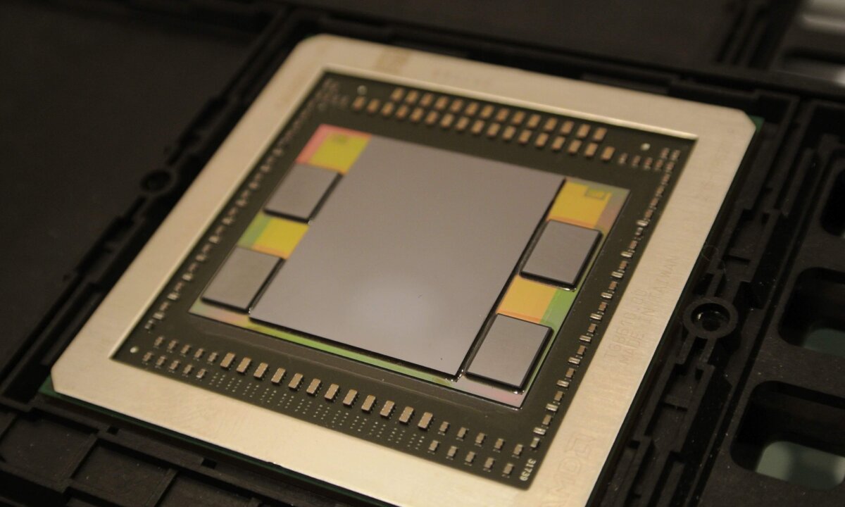
- AMD’s Bryan Black defined success as when they got the first product out the door that was part of a product family, not just a “one-hit-wonder. Based on the interview I had with Black back in July, I think we can safely say that by introducing the Fiji processor in its Radeon Fury product family, success has been achieved.
- Ehrenfried Zschech, Fraunhofer IKTS said that the impression he gets from this year’s conference is that the variety of 3D solutions is increasing and simultaneously the number of materials integrated in 3D stacks which brings new challenges to reliability and particularly requires study of thermal mechanical stress induced effects.
- On the supplier side, Hugo Pristauz, Besi, said last year that success would be when there are “no more headaches” with the die bond tool. Alignment accuracy and speed they’ve got covered, he said. “The tricky part is bond control.” After focusing on that for a year, he was happy to report that the bond control element is solved. While more challenges emerged, he says they have figured those out as well. “If I send my R&D guys to the customers, they can now achieve 100% yield.”
- Last year, Markus Wimplinger, EV Group, had three measures of success: a stack with memory on logic in a smartphone, stacked memory in servers, and hybrid bonding in volume production for image sensor technology. This year, he said that in terms of high-end applications, the memory stacks have appeared and that is a sign of success. “After hearing about all the efforts to optimize cost, we are on the road to success for the consumer products,” he added.
- Last year, Amkor’s Ron Huemoeller equated success with return on investment. He was happy to report than in the 2.5D product area, the company has products in production and have met their goals. The goal for next year is to go into production with SWIFT, the company’s advanced, high density fan-out technology. He also had said that when people are willing to design into it with faith, that will be success. And to some extent, that has happened.
- Saying that 3D IC is too expensive is not a good argument,”said Jürgen Wolf, Fraunhofer IZM, last year. “You could kill every good idea with this argument.” He predicted that reducing cost for TSVs and aligning technology specifications with the technology capabilities will bring 3D IC to success. He said he still believes this is true. Wolf says he sees potential for cost-efficent technology in production to accelerate integration into real products specifically for TSV. “It’s still important element in 3D integration,” he said. He noted that we also have to align with assembly techniques and look at the integration of the whole package. As an example, he talked about work they are doing to develop thin, micro-bumped stacks that don’t require underfill. He said they are working with Ziptronix to eliminate underfill. Additionally, there needs to be more collaboration with product designer .
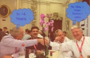 But the biggest question on my mind this year was, has anyone won the bet? Last year, Kevin Crofton, SPTS, bet Thomas Leicht, Lam Research, that there would be at least one memory on logic stack in production in four years time. The Stake: the best bottle of wine Thomas Leicht has ever had, Chateau Patreus.
When I asked them the status of the bet, Crofton wanted to know if HBM used in the AMD Fiji processor counts, because it has four memory die stacked with TSVs on a logic die. I was willing to say yes, but this is a pretty good bottle of wine, and we don’t want to be cavalier about what constitutes memory on logic. So let’s put it to a vote below in the comment section. Does it count? Or does Crofton have 3 more years to win? ~ F.v.T.


