


As it has in year’s past, the 2016 European 3D Summit kicked off with a market briefing. We heard from the usual suspects: Yole Dévéloppement (Rozalia Beica) and TechSearch International Inc. (Linda Bal). Additionally, in a nod to the business-centric tone of the conference, the committee invited Christian Knochenhauer, McKinsey and Company, to present on value creation in the packaging, assembly and semiconductor industry. Romain Fraux, System Plus, presented analyses of real products implementing TSV technologies, not only for the purposes of interconnect, to provide insight on the broader application of this technology.
While Knochenhauer’s presentation was rather sobering — apparently those packaging cornflakes realize higher profit margins than those packaging computer chips — It didn’t dampen the spirits of the attendees too much, as what was to follow was so much more optimistic.
Basically, according to Knochenhauer, the semiconductor industry is highly cyclical and under-performing (tell us something we didn’t already know). And only eight out of 188 firms in their database have performed consistently positive since 1996, while 115 companies have destroyed economic value. He also said there is no clear winning formula to generate value in assembly and test. Semiconductor is a winners-take-all industry (and I don’t have to list which ones are the winners.) However, he did say the smaller players in analog and capital equipment generate value by being market leaders in niche positions.
The market updates took a more upbeat turn, as Fraux, Bal, and Beica added to the growing list of real products that implement advanced wafer level packages, including FOWLP and 3D TSVs, as well as to the list of OSATS, IDMs and foundries that offer variations on FOWLP.
3D TSV in HVM
While Beica talked about the continuing trend of mergers acquisitions, she noted that 3D packaging is currently at the forefront of the semiconductor industry, as it offers faster time-to-market and allows for integration of all different functionalities in the same devices, which is difficult at advanced technology nodes, making More than Moore a more attractive option. Even the foundries are getting involved, she said. The bottom line is, the advanced packaging market is on the rise, and is currently dominated by flip-chip technologies. However, while 3D IC and FOWLP are both currently small markets, high growth is expected. Where there is growth, there is opportunity.
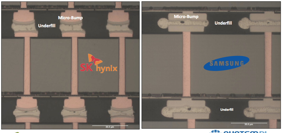
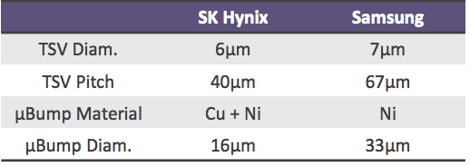
Gone is the speculation for whether 3D TSVs will be realized in high volumes. In his presentation comparing 3D TSV technology trends in memory, MEMS, and sensors, Fraux revealed that the finger print sensor on the iPhone 6s contains TSVs, and are the highest volume TSVs on the market, with 50K wafers produced. Other key players, as we know, are SK Hynix, with TSV in volume production in the HBM, and Samsung with its DDR4 memory. Raux presented detailed comparisons of both processes. In summary, he noted that processes for Samsung and SK Hynix’ stacked memory devices are close and share the same cost structure (Figure 1). Additionally, Beica declared that TSVs have gone mainstream for high-end computing applications. Figure 2 shows the roadmap for TSV product implementation.

FOWLP: Filling the Gap
Before diving into the FOWLP discussion, Bal talked about the increased numbers of wafer level packages (WLP) in consumer mobile products and wearable devices, driven by the desire for thinner products, as well as smaller form factor and low cost. “People think that thinner products are better, but this is a consumer perception,” she noted. “Thinner doesn’t make it work better.” Tear-downs of various smartphones resulted in an average of 5-7 WLPs per phone. WLP are also showing up in digital cameras and camcorders, laptops and tablets, medical and automotive devices, noted Bal.

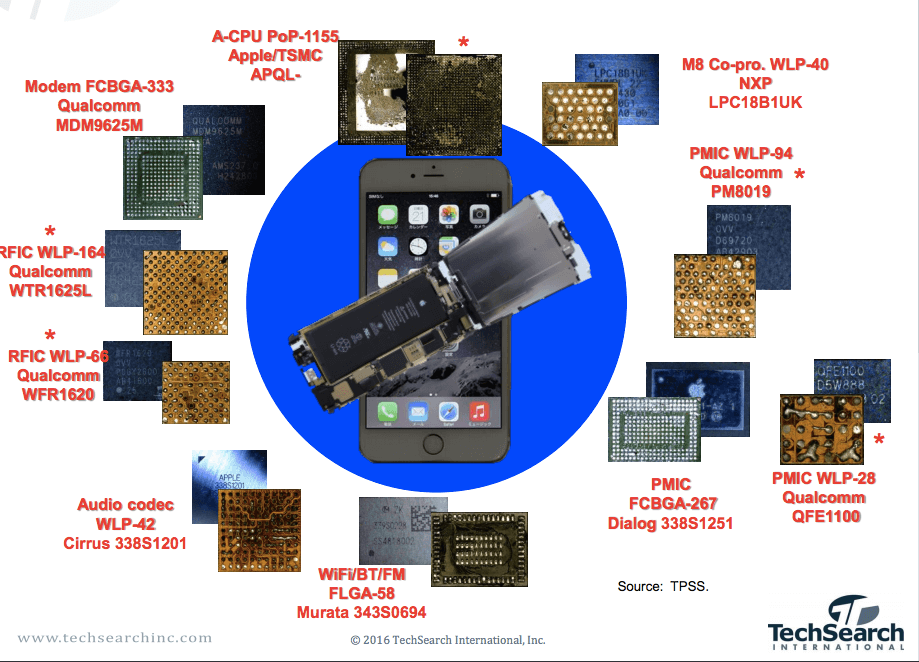
Drivers for FOWLP are similar to WLP, with the added benefits of being able to achieve finer line/space than conventional WLP, accommodate die shrinks, and allow for multi-die integration. When FOWLP is implemented in the bottom package of package-on-package (PoP) configurations, the result is a lower profile package with high routing density that enables system integration at a competitive cost. According to Bal, this is why FOWLP is being rapidly adopted into consumer mobile applications to fill the performance gap between WLP and interposer and 3D ICs (Figure 3).
Both Bal and Beica detailed OSAT activities in FOWLP, and talked about conventional approaches, alternatives to reconstituted wafer, and and new developments for high-density fan-out. They also both reported that the mobile and wireless markets are the primary markets for FOWLP, and that it’s also starting to be adopted into automotive and medical markets. For example, in automotive applications, it’s being adopted for mmWave radar for advanced driver assist systems (ADAS).
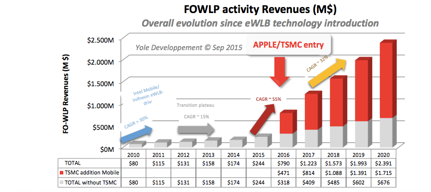
According to Beica, the entry of Apple/TSMC into the FOWLP space caused Yole to adjust its forecast of CAGR for the 2014-2016 from 15% to 55%, with and additional jump of 32% between from 2016-2020. Additionally, Beica predict that the market for FOWLP will exceed $2B by 2020 (Figure 4). TechSearch International Inc. predicted an overall CAGR for FOWLP of 87% from 2015-2020.
A few Words on SiP
One of the advantages of all varied advanced WLP platforms — wirebond, FC, embedded, 2.5D and 3D — is that together, they enable system-in-package (SiP) platform. Beica defined SiP as two or more components with different functionalities packaged into a system or sub-system. She explained that SiP allows for smaller form factor, more flexibility, and more technology integrated into the same package, resulting in higher performance, faster time-to-market, lower cost, IP protection, and higher added value. It suits various markets including wireless communications, consumer, automotive, medical, and IoT. Beica noted that SiP already dominates smartphone platform, with many growth opportunities.
All in all, it seems that after years of anticipation, advanced packaging’s importance to the industry is being acknowledged. No longer is it the necessary evil – it is a value-add. This set a positive note for the remainder of the conference, and set the perfect stage for the remaining presenters to tell their stories. ~ F.v.T


