


At last week’s sixth annual IEEE 3D Test Workshop, it was exciting to see the number of presentations that demonstrated solutions to the 3D test challenges that have been plaguing us for so long. Not only that, but these 3D test flows are being used on real 3D integrated devices available on the market such as Xilinx Vertex FPGA product line, SK hynix’ high bandwidth memory (HBM) stacks, and AMD’s Fiji-based products that for the first time incorporate both interposer integration and HBM in one 3D system.
However, a test workshop wouldn’t be worth the registration fee if it didn’t send off its attendees with a whole new set of challenges to tackle. These are test engineers, after all. The fun part for these guys isn’t finding out that all the issues are solved, It’s finding out what lies ahead. The savvy workshop organizers know this is what fills the seats. They didn’t disappoint – day two of the Test Workshop featured an entire session on Monolithic 3D, including an invited talk by Zvi Or-Bach, founder and CEO of MonolithIC 3D, and well-known monolithic 3D evangelist; and a panel discussion moderated by yours truly and featuring panelists Or-Bach; Bob Patti, Tezzaron (because no panel I moderate would be complete without Bob on the panel); Sandeep Goel, academician and senior manager, TSMC; Yang Du, Director of Engineering at Qualcomm; and Sebastien Thuriés, researcher, CEA-Leti.
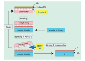 Or-Bach kicked things off with a 15-minute presentation on a modification of a 20 year old process, ELTRAN (epitaxial layer transfer), that he says could help propel monolithic 3D ICs past the hurdles of high temperature processing. By definition, monolithic 3D IC is a sequential build up process that uses traditional front-end lithography processes to create stacks of transistor layers, vs. stacking complete die or wafers using through silicon via (TSV) technology. Currently, the monolithic approach is limited to two layers due to the high temperatures (above 400°C) required to process transistors. Or-Bach explained that the ELTRAN process extends monolithic 3D beyond its 2-layer limit by adding subsequent layers of circuitry that are cut from a pre-processed donor wafer fabricated using traditional high-temperature transistor processes, that can then be sent back for rework and reuse. He noted that this approach also allows for vertical heterogeneous integration, as the layers can comprise disparate technologies such as analog, logic, and memory.
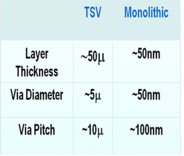 Or-Bach’s definition of monolithic 3D is looser than others. While most maintain that it is a sequential build-up processes rather than parallel, he distinguishes monolithic 3D from 3D TSV as having 10,000x the vertical connectivity TSV, and is measured in nanometer scale vs. micron scale. Thuriés noted that Monolithic 3D provides ultra high density integration : x104 vs. Cu-Cu or HD-TSV.
Patti pointed out that the Eltran process is essentially the same as Tezzaron’s layer stacking process and is not sequential, so is also not a monolithic approach. Yang Du, further complicated the definition by referring to monolithic 3D as 3D VLSI, defined as ”Fab driven 3D integration technologies that allow functions to be synthesize and integrated in all physical dimensions monolithically and seamlessly as conventional VLSI.” Leti’s Coolcube is an example of this.
Goel noted that monolithic 3D’s bottom layer differs from other layers in-terms of transistor type/quality. Additionally, upper layers have strict requirements on temperature and thermal stress for the whole stack. Ultimately, Or-Bach urged attendees not to get caught up in what we call it, but rather what it achieves.
Or-Bach said that 3D NAND is an example of where it is already in volume production for memory. However, a monolithic approach for logic has yet to be commercialized. As previously stated, 3D TSV products are now in production in many high computing products, and in HVM in image sensors. Whether it beats 3D TSV to consumer products is yet to be determined.

As this was a test workshop, discussion turned to the test advantages and challenges of the monolithic 3D approach. Thuriés noted that because it’s a sequential process, pre-bond tests are not required. However, design for test is a challenge, because while its full scan 2D compatible, it requires scan re-order for multi-layer optimization that will require EDA support. Thuriés suggested that test standardization might be in order. Or-Bach’s take was that high integration with multiple strata will drive two new test related requirements: contactless wafer-“These new testing capabilities would support repair, rework, redundancy and in-line process monitoring and control,” he noted.
Goel offered a laundry list of test challenges. If you go with the ‘no known-good-layer concept, you may continue to build the stack without realizing that it doesn’t work. To establish known good layer requires changes in the DFT scheme to accommodate for the partial circuit. Surface preparation for possible bare layer probing could be required. And what about a quality metric for layer-level test? Then there’s the issue of process variation between die. Bottom line, “f you thought 3D test was difficult and expensive, think again: M3D test will surpass all limits,” he noted.
So there you have it. Test guys roll up your sleeves! There’s work to be done! ~ FvT


