Whenever Francoise organizes an event, she always manages to compose a mixture of entertainment, real work and valuable education. This panel was no different. Francoise moderated the IWLPC 2015 Panel Discussion: Interposers, 3D TSVs, and Alternatives: What are the Options and Where do They Fit? featuring Aric Shorey, Corning, Inc.; Thibeault Buisson, Yole Developpement; Hughes Metras, CEA-Leti; and Mike Kelly, Amkor. It started with twelve Kahoot questions to engage and challenge the audience on their knowledge of alternatives to 3D TSVs in the packed-full conference room. If you are not familiar with the Kahoot game, check it out at getkahoot.com for a description. The winner who gave the correct answers the fastest, was Dave Towne, formerly at Cisco, now working for Yole. (To test your own knowledge or review the questions take the quiz yourself here.
While the panelists, Shorey, Metras, Kelly, and Buisson were interested observers in part 1, Francoise really put them to work in part 2, first with introducing themselves, their companies and product focus.
Aric outlined Corning’s commitment to Glass Interposers and highlighted some of the benefits of glass: In addition to their low cost, Glass Interposers are stiffer than organic material, have less surface roughness, can offer down to 2/2µm line/space pitches, can be manufactured with a wide range of Thermal Coefficient of Expansion (CTE) to match silicon (CTE= 3 to 4) and organic substrates (CTE above ~ 12) to avoid thermo-mechanical stress and resulting reliability problems. Last, but not least, glass serves RF applications very well, due to its low insertion loss.
Thibeault outlined the role of Yole in the electronic components industry, especially their focus on packaging technology for ICs, MEMS and Sensors for use in electronic systems.
Mike briefly outlined the progression of single-die packaging technology, then the development of multi-die packaging solutions in the latest 10+ years.
Hughes, as CEA-Leti’s US representative, listed a number of high-profile developments Leti is working on, together with major customers: He explained Leti’s monolithic 3D-IC program, trademarked “CoolCube” and Leti’s progress towards a multi-layer process with a very low temperature profile, to not degrade the performance of previously manufactured layers of active and passive circuitry. Hughes also emphasized that, compared to TSV/micro-ball interconnects, the vias in monolithic 3D-IC are magnitudes smaller and enable many more interconnects, at much lower interconnect power.
After these brief introductions Francoise opened the floor for questions – related to the Kahoot questions and other topics.

- What are common interposer materials and why? Thibeault responded to Aric’s list of glass benefits and mentioned that glass is not as popular as Silicon and Organic are at this time.
- What is a good package for high performance? Kelly suggested to consider Amkor’s SLIM, TSV-less technology. Shorey emphasized that a glass interposer solution is best for very high frequencies and useful for many other applications. Buisson added that glass is used for packaging MEMS, because it seals very well hermetically. Aric stated that glass is being process in wafer- or panel form today. Even lower cost processing of glass roles will be made available in future.
- Metras raised an important point for Silicon Interposers – their ability to implement passive and active components. Leti is developing, with iPdia, I/Os, ESD circuitry, Power Management Circuits (PMICs) and other active and passive circuits to remove this kind of large area, noisy and high power circuits, especially from sub-20nm chips, to reduce total unit cost. Kelly confirmed that he also sees a trend to active silicon interposers. Hughes added that silicon interposers, when used for electrical/optical applications, can also implement the needed wave-guides.
- When asked which interposer material is best in pulling heat out of an IC, Kelly explained that heat typically travels vertically, up into a heatsink and down into the PCB. Conducting heat horizontally, is primarily done by the copper traces. Organic interposer have thicker copper traces than glass or silicon, therefore distribute heat better across the interposer and package, minimize problems caused by local hot-spot.
- Are the initially aggressively hyped 3D logic stacks finding market acceptance? Kelly explained that very high bandwidth and high-speed applications justify the challenging vertical stacking of logic dies. Buisson added that for integrating heterogeneous functions (e.g. image sensor and processor, MEMS and logic,…) vertical stacking is getting common now. Kelly reminded us that SONY’s 40+%t market share in cameras for phones, tablets and other devices today is due to the small footprint SONY’s vertically stacked sensor & processor configurations allow.
- What’s the best package type for applications like very thin smart phones? Quick answer: It depends! For lower pin counts fan-In packages are clearly the thinnest solution, emphasized Thibeault, and mentioned that today’s smart phones utilize many ICs in FI-WLP. For higher pin counts Fan-Out packages fit the bill, like TSMC’s integrated Fan-Out type, branded InFO.
- In response to my obligatory question: “How supportive are EDA vendors?” I heard that Cadence and Mentor as well as several smaller EDA vendors are working on evaluating test vehicle to solve modeling challenges and are, jointly with suppliers and customers, developing design solutions for IC- and package designers. However, the complexity of the challenges requires more joint efforts, before a high-productivity and user friendly die-package-board design flow will be available. Metras added that Leti’s customers use a broad range of tools and need all their EDA partners’ support.
- How about standards in this field? Kelly mentioned that Amkor’s customers, when stacking logic and memory, rely on JEDEC’s Wide I/O 2 standard. Also, the interposer-based CPU/GPU and High-Bandwidth-Memory (HBM) combinations can rely on the JEDEC standard for HBM. Shorey added that SEMI published a number of standards for manufacturing flows. He also highlighted that glass manufacturers can leverage their experience with optics and flat panels to develop glass interposers and support their users.
The very experienced panelists offered good answers to all the audience’ questions, but clearly showed that additional development work is needed. Last, but not least, the audience demonstrated that a lot of additional education is required before project managers and individual designers will be confident enough with 2.5 and 3D technology to rely on it for a major program, facing a tight schedule.
Every new technology I was involved in rolling out had to prove itself on smaller, less schedule-driven opportunities first. Only when a company was ready in time to win major opportunities from advanced customers, could it reap the benefits of strategic thinking and investing in their people and equipment.
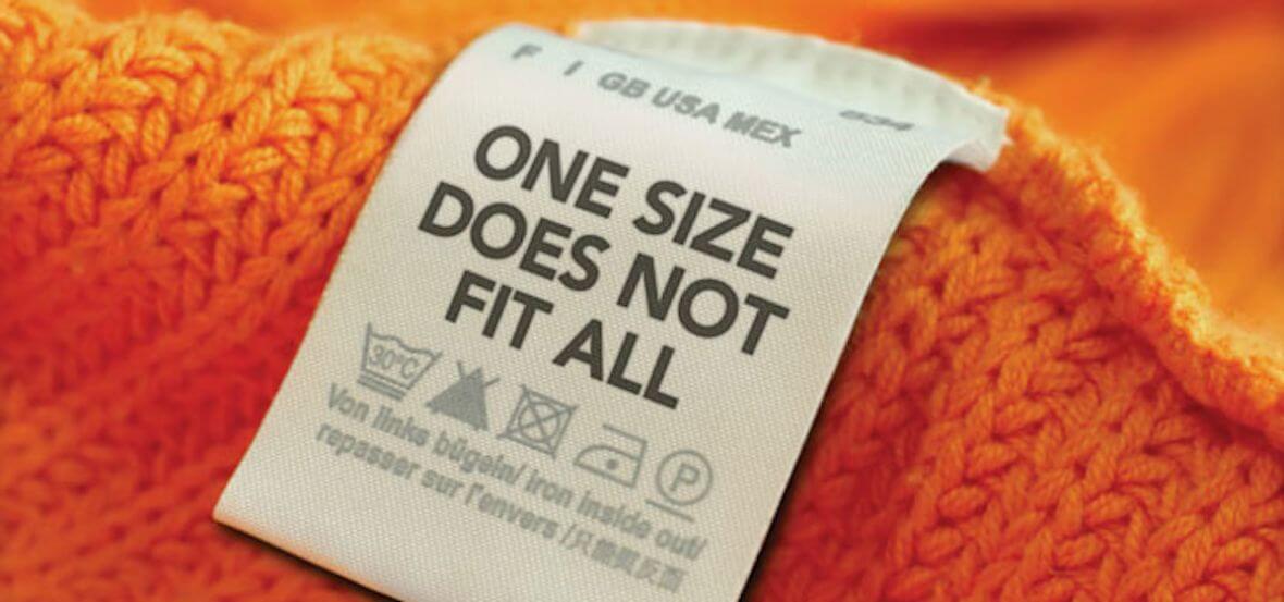
During the panel the comments “ It Depends” and “One size doesn’t fit all” were mentioned many times. Which 2.5 or 3D solution fits which opportunity is the most important first step towards making money with these new and promising technologies. It won’t be an easy step, but following Moore’s Law fits fewer and fewer opportunities! ~ Herb, 10/15