On Thursday, September 17, I was invited to attend TSMC’s Open Innovation Platform (OIP) conference, that showed TSMC’s rapid progress and the power of TSMC’s Grand Alliance. As a former Alliance Manager, I really enjoyed seeing how TSMC’s far-reaching vision and strategic alliances, combined with excellent execution and customer service, made them the largest wafer supplier to fabless IC vendors, fab-lite companies and IDMs.
Actually, I should be very mad at TSMC, because they systematically eroded my product lines’ ASIC business when I worked at VLSI Technology and “motivated” me to leave VLSI. I changed to an EDA company, ViewLogic. During my year at ViewLogic I practiced “if you can’t beat them, join them” and started joint efforts with TSMC in 1997. When Synopsys acquired ViewLogic, I got the opportunity to broaden this cooperation significantly and was able to accelerate TSMC’s growth with the first reference flows and broaden the use of Synopsys tools at the many emerging fabless IC vendors. A clear win-win.
Why am I boring you with part of my life’s story? Because TSMC is the perfect example of a company that not only talked about their plans for and likely benefits of a Grand Alliance, but also executed this winning strategy very well. The recent OIP event demonstrated even better than in previous years that only with partners, in a well-managed EcoSystem, customers can take advantage of TSMC’s process technologies, down to 7nm, and the vast wafer fab capacity.
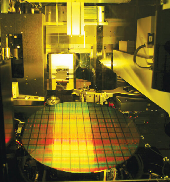
After more than 20 successful years as wafer foundry following Moore’s Law, TSMC showed again last week that they have expanded their capabilities beyond the smallest feature sizes needed by a declining number of very high-volume customers.
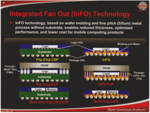
TSMC has also developed ultra-low power technologies for IoT edge nodes, high-voltage processes for automotive, as well as MEMS and Sensors for a wide range of applications. Expanding even beyond wafers, TSMC has invested in packaging technology. After introducing Chip on Wafer on Substrate (CoWOS) technology in 2012, TSMC developed a very thin and low cost IC packaging technology, called Integrated Fan Out (InFO) to meet the needs for thinner single- and multi-die ICs (Figure 1). Several, usually reliable, sources told me that the A10 application processor in Apple’s iPhone 7, to be introduced in Fall 2016, will be taking advantage of InFO. This will encourage Apple’s many IC vendors to match Apple’s thin Application Processor (AP) and use InFO or equally thin packages utilizing chip-scale packaging or Interposer solutions.
InFO technology is being considered for many other applications. To educate IC- and package designers at the many adopters, Cadence’ William Acito presented InFO Design Challenges and Methodologies in the EDA portion of the OIP event. The slides he presented are in the partner handout, starting on page 48. This handout also includes presentations delivered by the other major EDA partners, ANSYS, Mentor Graphics and Synopsys. TSMC’s Grand Alliance also includes many IP partners. Analog Bits, ARM, Cadence, Imagination, Snowbush and Synopsys got the opportunity to present in the IP Track. The Services Track also included EDA and IP Vendors. Presenters from Dolphin, eMemory, GUC, Kilopass, M31 Technology, MediaTek, Sidence, Synopsys and Xilinx outlined their contributions to TSMC’s Grand Alliance.

A number of customers presented how they benefit from TSMC’s strengths and its many partners. Avago and Xilinx complemented Cliff Hou’s morning presentation, HiSilicon, MediaTek, Oracle, Qualcomm, and Semtech amplified partners’ presentations in the afternoon. When you read this you probably have, like me, already seen what several other OIP conference attendees reported about this impressive event. Instead of duplicating in detail what these attendees wrote, let me put what I captured, in bullet form, in the context of key market requirements:
- Steps to lower cost
- TSMC’s low cost FinFET alternative, 16 FFC, uses fewer masking layers versus 16 FF or 16 FF+ and lowers tooling cost. Fewer masking layers, especially the reduction of double-patterning steps, reduces variability, improves yields and lowers actual unit cost.
- TSMC’s 10nm process shrinks transistors and metal system and will reduce die area by slightly more than 50%.
- Based on a 7nm SRAM test chip in progress, TSMC projects another 40 -45 %die area reduction.
- The billions of IoT peripheral nodes to be installed in coming years will need extremely low-cost and low-power circuits. TSMC reached back in time and converted mature technologies into ultra-low power (ULP), low cost processes, in 55 and 40nm, both in production now. A 28nm ULP process is ramping this year.
- As outlined above, TSMC’s InFO packaging technology is a very important step towards lowering total unit cost.
- Steps to reduce power dissipation
- 16 FF+ consumes 70% less power than 28 HPC at the same performance.
- TSMC’s 10 nm FinFET technology consumes 40% less power than 16nm.
- TSMC expects that their 7nm process will reduce power by another 35 – 45%.
- All these steps following Moore’s Law improve performance, at constant power, typically by a similar percentage.
- TSMC’s ULP processes operate now at 0.9V (55 and 40nm) or 0.7 V (28nm). A 0.6 V version for 40nm is coming up.
- 16 FFC will be characterized down to 0.4 V to serve ultra-low power, lower performance applications.
- Considering that I/O power dissipation of single-die ICs can be up to about 30% of total IC power, multi-die integration, like TSMC’s CoWoS and InFO packaging technologies allow you to minimize the number of high-power I/Os and with it, reduce total chip power significantly.
- Integrating heterogeneous functions in one IC package
- In addition to IoT, Automotive and Consumer applications require a multitude of MEMS to sense physical and biological parameters. TSMC offers MEMS for sensing motion and pressure as well as backside illuminated (BSI) image sensors.
- If an application (e.g. Automotive) requires high-voltage, TSMC’s BCD and GaN processes fit the bill, up to 650 Volts.
- – Just like CoWoS’ and InFO’s lower I/O power dissipation, these multi-die packaging technologies simplify integration of heterogeneous functions, each implemented in the most cost-effective process technology in one IC package.
- IC form-factor, especially for very thin mobile devices
- Mobile devices need to be thin to fit into the back pockets of the tightest jeans. TSMC’s InFO technology offers much lower package height than other available IC packages. As the TSMC slide (Fig 1) highlights, InFO meets this important requirement and, compared to the already thin flip-chip technology, reduces package height significantly.
- Lowering the entry-barrier as well as mitigating design- and supply-chain risk
- The rapidly increasing number of design rules, the need for double-patterning at 16 and triple-patterning at 10nm, much higher variabilities, increasing interconnect delays, localized heating and electro migration challenges are just a few of the hurdles today’s IC designers need to reckon with.
- TSMC’s 2015 CapEx of $10.5 – 11B will assure that both capability, as well as needed manufacturing capacity will be in place, as customers tape out and ramp designs in these advanced process technologies.
- TSMC plans to also invest $ 2.2B in 2015 in R&D to expand their design enablement capabilities. TSMC offers more than 200 Process Design Kits (PDKs), thousands of tech files, IP blocks and a number of up-to-date IC- and package reference design flows. Many Ansys, Cadence, Mentor, and Synopsys tools are already qualified down to 10nm.
- The many partner presentations late morning and all afternoon, as well as the available experts from technology partners in the exhibition area, demonstrated the broad support TSMC customers can rely on while designing chips, ramping up production, improving yields or driving other cost-reduction effort with TSMC.
As the recent mergers and acquisitions wave in the semiconductor industry has shown, our industry is maturing. Differentiation and the resulting higher margins are much more difficult to achieve. Also, IC design is very lengthy, costly, and risky. Many executives I talk with prefer strong partnerships over getting acquired or having to explain to Wall Street why they want to buy another firm. TSMC’s track record as an innovative and trust-worthy partner and their Grand Alliance may also be your ticket to future success and independence. ~Herb