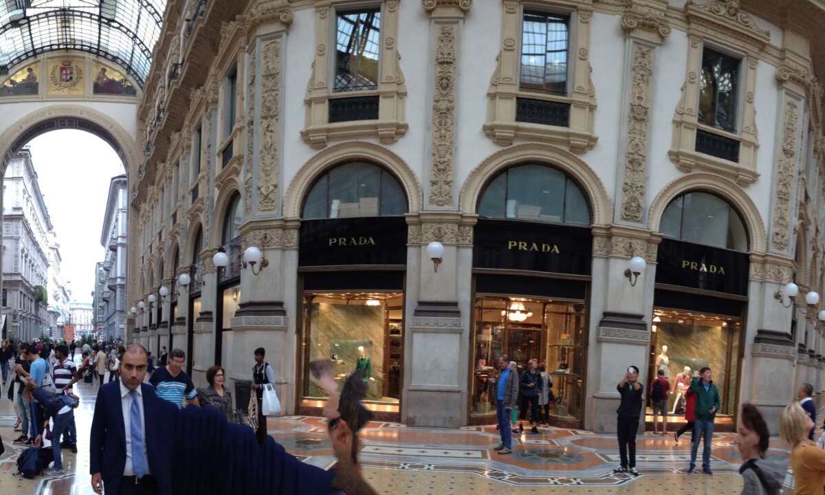
Last week, (September 18-19, 2015) SEMI Europe hosted its first-ever European MEMS Summit, in Milan Italy. It was a fitting host city for several reasons; first, the nearby EXPO 2015, which focused on Feeding the Planet – Energy for Life, inspired the theme of the MEMS Summit: “Sensing the Planet, MEMS for Life.” Second, it seemed that in comparison to the semiconductor industry, which calls for a rapid-fire 2-year turnaround for next-node silicon based on Moore’s Law, MEMS development has always enjoyed the Italian, Dolce Vida approach. Much of the topic of discussion over the course of two days centered on ways to help the MEMS industry speed up the development process, or alternatively, accept the time-to-market as standard and instead work towards developing the next killer app.
The event exceeded SEMI’s original expectations, as it drew speakers and attendees not only from Europe but from around the globe to discuss what MEMS and sensors bring to our life. I was invited by SEMI to attend, as MEMS is critical to heterogeneous integration; one of the areas we’ve been talking about because 3D integration is an enabler of MEMS integration.
First, the numbers: Final tally brought the attendee count to 260 attendees representing 21 countries. The conference featured four keynotes, 15 invited talks, 28 exhibitors, 18 sponsors, and 9 media partners. Participants hailed not only from the MEMS industry but the semiconductor industry as well, which supported the notion that meeting the goals ahead of us will require great collaboration across the semiconductor and MEMS supply chain.
While the official theme of the event was Sensing the Planet – MEMS for Life, the presentations and ensuing discussions unearthed a number of sub-plots to the story. One was the story about how MEMS is “snagged on the hook of one product, one package, one process, which could potentially be a problem going forward,” noted EE Times Peter Clark, during his wrap-up of the conference.
Peter Merz, X-Fab, noted that this dilemma is partly due to the fact that many customers without MEMS experience are defining MEMS products. He said it’s too expensive to have so many products without a critical market size. It leads to unstructured development and poor process flow quality. The ROI for capacity and capability expansion is not attractive for only one product. “The general value chain is easy but typical issues and problems make it messy,” he said.
The end game for semiconductor development has always been to cram more transistors on a chip. In MEMS, the end game is to create a new capability that addresses a real-world problem, not just getting more performance, speed, and processing power out of a chip.
Unfortunately, this fragmentation leads to 5-10 year product development cycle time, which many feels is too long to meet today’s market requirements. Some say CMOS doesn’t have that luxury because it has to comply with Moore’s Law and adhere to a 2-year cycle time for new products to stay in the game.
We are expecting, according to Sean Ding, Chief Scientist in the Sensor Solution Lab at Huawei, a need for 500-5000 new sensors in the next five years. “I need them yesterday. I have applications waiting for them,” he said. He was sporting a number of prototype wearable devices – a fitness tracker that also converts to a Bluetooth headset to set it apart from the competition, and a smart watch that needs an energy harvester to increase its battery life to “one year” to make set it apart.
Pascale Langlois, CEO Tronics, offered 3 key success factors to overcome time-to-market barriers that create more value in sensors and MEMS and allow for simpler industrialization. First are people with the skills to follow fast market transitions and meet customer requirements. Next is technical expertise to develop re-usable and proven technology blocks that help standardize the platform. Lastly, it requires tighter relationships within the value chain and manufacturing flexibility: i.e. a local source of supply with responsive, proactive, and knowledgeable technical support. Ultimately, he said, accelerating the innovation cycle for product development requires collaboration across the whole ecosystem.
To be successful, Merz recommends a balanced mix of single capacity, module technology, and an open process platform. This calls for a strong MEMS development team, and a balanced production mixing volume vs. cost. Additionally, strategic alliance with both customers and industry research partners is a must.
“MEMS applications are drivers and may seriously limit innovation when we squeeze them into standard platforms,” cautioned Merz. “Expect long trajectory from idea to revenue.”

Benedetto Vigna, Executive VP and general manager, ST Microelectronics, called for “Leonardo-like” MEMS engineers and Renaissance managers who are lateral thinkers. “It’s not about time, it’s about the return you can get. There’s a big difference between MEMS and CMOS,” he noted.
VIgna also talked about “Smart Things” as a market driver. “We can see movement, but we’re not sure yet if it will be the same movement as the smartphone.” He added that smart things cause disruption in a business model by transforming the meaning of an object. MEMS can help by adding sensitive features to an object. Ultimately, he said, Smart Things allow us to do more with less. For example, there are sensors to help reduce water consumption, or sensors being put in lights to lower power consumption.
With approximately 300 competitors developing similar wearables for the consumer market, Ding says the industry needs a disruptive product. “I wish you guys could help me do that,” he said. Ding said “The hockey stick is 2015. The sensor industry will experience high growth. Don’t wait and leap forward. Run as fast as you can.”
Huawei’s presence at this event further proved that China is hot to expand into the MEMS Market. Peter Himes of SITRI talked about the country’s increased efforts to become a more substantial player in the MEMS space. “The goal is not to make MEMS happen in China, but to make the MEMS ecosystem work more efficiently everywhere,” he explained. “The message we are sending is that innovation happens everywhere. You shouldn’t have to move to Shanghai to pursue your dream.”
“We are living in Golden Age of MEMS technology. We have the opportunity to create value, and create wealth,” noted Clark. He cautioned, however, to be careful not to put too many eggs in the wearables basket. “Wearables are a technology looking for a problem,” he said. “Be careful not to believe your own hype.” Instead, he suggests focusing on technology that is more useful. People wear things because they have to: such as eyeglasses, hearing aids, for sports, or medical reasons. These are the more sustainable applications, and when balanced with automotive and industrial applications, may be what really takes MEMS into high volumes.
All in all, it was an inspiring two days, with lots more to tell. And if you missed this year’s event, make a note to attend next year’s event in Stuttgart, Germany. We’ll let you know when as soon as we know. ~ F.v.T.


