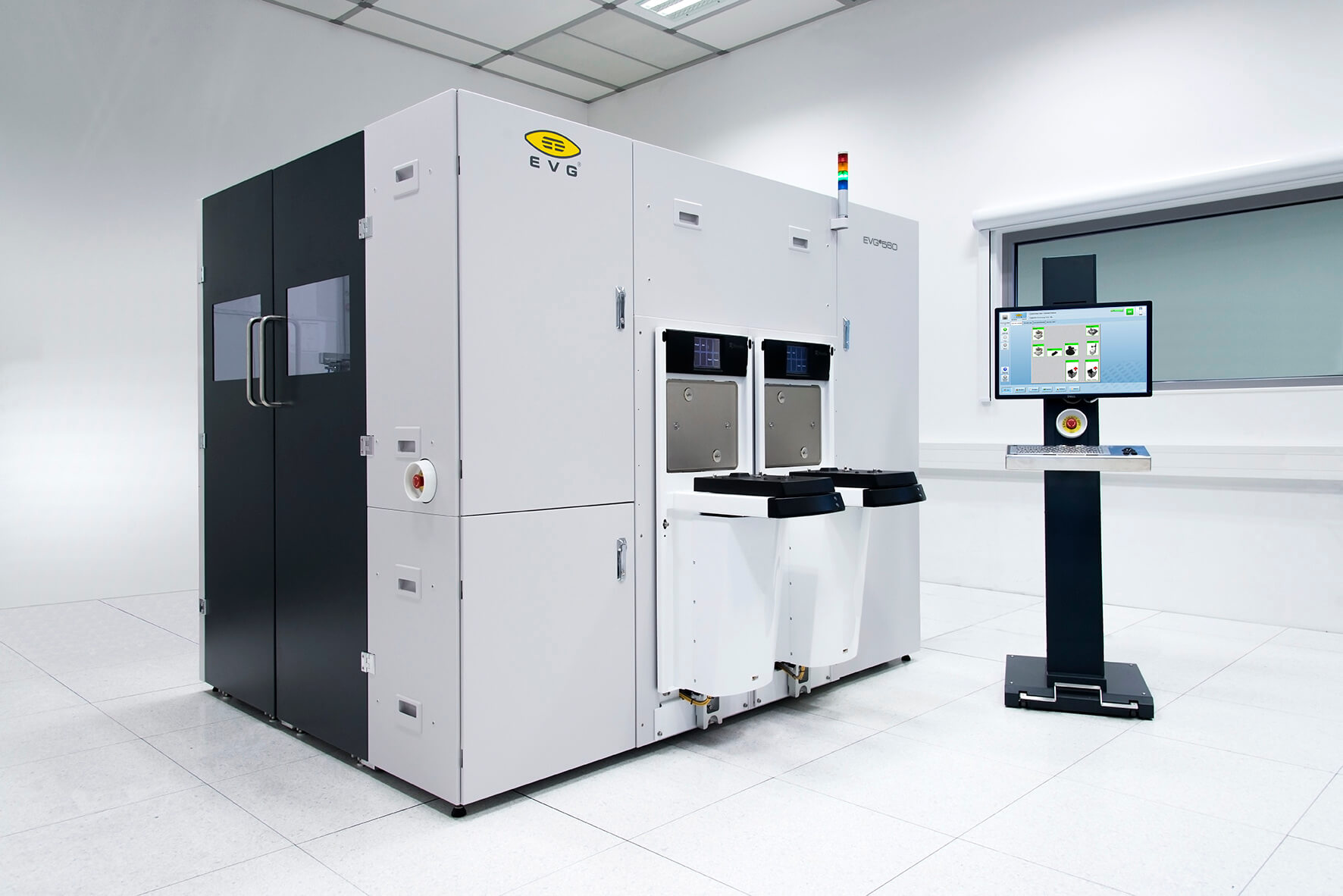
 ST. FLORIAN, Austria, August 31, 2015—EV Group (EVG), a leading supplier of wafer bonding and lithography equipment for the MEMS, nanotechnology and semiconductor markets, today announced that the company is experiencing strong demand for its automated 300mm polymer adhesive wafer bonding systems. Over the past 12 months, the company’s order intake has doubled for these systems, including the EVG®560, GEMINI® and EVG®850 TB/DB series of wafer bonders. This includes multiple system orders from leading foundries and outsourced semiconductor assembly and test (OSAT) providers headquartered in Asia. Much of the increase in demand is being fueled by advanced packaging applications, where manufacturers are ramping up production of CMOS image sensors as well as vertically stacked semiconductors incorporating 2.5D and 3D-IC through silicon via (TSV) interconnect technology.
According to market research and strategy consulting firm Yole Développement, the equipment market for 3D-IC and wafer-level packaging (WLP) applications is expected to grow significantly, from $933 million in 2014 to $2.6 billion in 2019 (total revenue), at a compound annual growth rate (CAGR) of 19% over the next five years*. Adhesive wafer bonding plays a critical role in supporting these applications.
Automated adhesive wafer bonding enables high yields on stacked devices
Adhesive wafer bonding is a technique that uses an intermediate layer (typically a polymer) for bonding two substrates, which is an important process technology for advanced packaging applications. The main advantages of using this approach are low temperature processing, surface planarization and tolerance to wafer topography. For CMOS image sensors, polymer adhesive bonding provides a protective barrier between the surface of the image sensor and the glass cover wafer. For 3D-IC TSV applications, polymer adhesive bonding plays an important role in temporary bonding and debonding applications, where product wafers are temporarily mounted on carriers with the aid of organic adhesives to enable reliable thinning and backside processing.
For both CMOS image sensor and stacked memory/logic applications, fully automated wafer bonding solutions are essential to support manufacturers’ migration to larger (300-mm) wafer substrates to lower their overall cost of production. For example, minimizing total thickness variation (TTV) of the adhesive layer after bonding is crucial in defining the final product thickness tolerance. This ultimately has an impact on enabling thinner wafers and devices, which in turn enables higher interconnect densities and lower TSV integration costs. EVG’s automated wafer bonding systems provide superior control of TTV and other parameters through repeatable wafer-to-wafer processing and integrated inline metrology to monitor TTV throughout the bonding process. As a result, manufacturers are increasingly turning to EVG to support their automated wafer bonding needs.
“We’ve truly entered the era of 3D-ICs, with demand for TSV wafers rising on a number of fronts—from CMOS image sensors for smart phone cameras and automotive surround view imaging, to 3D stacked memory and memory-on-logic to support high-performance, high-bandwidth applications such as networking, gaming, data centers and mobile computing,” stated Hermann Waltl, executive sales and customer support director at EV Group. “Automated wafer bonding is a critical process for supporting the volume manufacturing needs of CMOS image sensor and semiconductor device makers addressing these applications. EVG has invested years in the development of wafer bonding technology to make it a critical value-add solution for the advanced packaging market. Our breadth of knowledge in wafer bonding equipment and processes—along with our strong network of supply chain partners—has positioned us well to anticipate future industry trends and develop new solutions that meet our customers’ emerging production requirements.”
About EV Group (EVG)
EV Group (EVG) is a leading supplier of equipment and process solutions for the manufacture of semiconductors, microelectromechanical systems (MEMS), compound semiconductors, power devices and nanotechnology devices. Key products include wafer bonding, thin-wafer processing, lithography/nanoimprint lithography (NIL) and metrology equipment, as well as photoresist coaters, cleaners and inspection systems. Founded in 1980, EV Group services and supports an elaborate network of global customers and partners all over the world. More information about EVG is available at www.EVGroup.com.

Contacts:
Clemens Schütte
Director, Marketing and Communications, EV Group
Tel: +43 7712 5311 0
E-mail: Marketing@EVGroup.com
David Moreno
VP, MCA, Inc.
Tel: +1.650.968.8900, ext. 125
E-mail: dmoreno@mcapr.com