


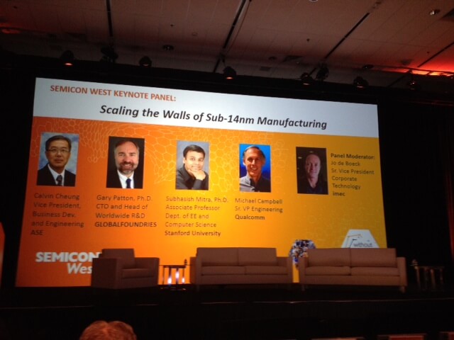
I almost didn’t attend the keynote panel titled, Scaling the Walls of Sub 14nm Manufacturing, at SEMICON West last week, because in my experience as a blogger/journalist focused on advanced packaging, interposer integration and 3D ICs, discussions on scaling rarely talk about packaging. In fact, up until now, it’s been an either/or discussion. Either we scale further, OR we look at stacking as an alternative. But then I noticed the panel line-up included Calvin Cheung, ASE, and Mike Campbell, Qualcomm, along with Garry Patton, Globalfoundries and Subhasish Mitra, Stanford University, and monitored by imec’s Jo de Boeck, and thought just maybe I should check it out; and I’m so glad I did.
It became clear early in the discussion that we can no longer talk about scaling below 14nm without also talking about the implications for packaging. 3D is now a given, and its become part of the overarching conversation, rather than being relegated to its own little box.
“This is a team sport now,” noted Patton, “We are working closely together (with OSAT partners) from early research to volume manufacturing.” While Patton said he’s not worried about solving the physics of scaling beyond 14nm, he is concerned about scaling in such a way that they can deliver a value-added product to their customers. Designs are costly, and it’s tough to get 50% cost improvement. He sees interposer and 3D integration as exciting areas that allow different thinking in terms of scaling.
The reality is, to address yield issues that come with further scaling as well as packaging challenges requires a system-level approach. From Qualcomm’s perspective, noted Campbell, the whole system needs to be interactive between the package, system, and silicon from the R&D stage to avoid having gaps in the system.
Mitra concurred, stressing that we need to get away from linear thinking and apply nano-systems thinking in technology development. “How do I put them together in a dense fashion?” he asked. “Using extreme scales of 3D integration.” MItra says we have the opportunity for 1000x in energy efficiency.
Offering the OSAT perspective, Cheung talked about the importance of chip/package interaction (CPI) and how with interposer (2.5D) integration, OSATS are now dealing with approximately 200K interconnects. “Can the OSAT industry provide interconnect technology to support those needs in a cost effective way?“ he asked.
Additionally, Cheung noted that the business model is becoming a challenge because OSATS have to support silicon coming from different major foundries, and managing cost and yield becomes daunting, particularly with the rapid product life cycles of mobile products. “Robust yield has to happen from the get go,” he noted. “How do we come up with a new model working with foundries and design houses? We need a methodology so that we have good yield within the first month.”

Campbell noted that while today foundries provide PCM data to keep the design community safe from internal variability, he doesn’t see that working over the long term. “Solving yield requires understanding the system,” he noted. He called out KLA Tencor’s metrology tool, saying it was “a wonderful tool” for inspecting wafer-level stacks and monitoring defects – determining which are killer defects and which can be worked on later. The only thing missing is data transfer to the packaging team to help understand the yield curve. He used this example to stress the need for the same level of interaction with the packaging houses and create design rules up front. “Without the package we don’t get to market,” he noted, adding that metrology companies have a pivotal role to play in all this, and need to communicate on the same level across disciplines to meet the challenge.
Campbell echoed Patton’s declaration that semiconductor manufacturing has indeed become a team sport where everyone needs to speak the same language. He said the complexity factor requires tools – even those from different tool manufacturers – to have a common language and data output for rapid and systematic data mining.
For the OSATS, noted Cheung, it’s been a team sport for some time. “We pride ourselves in being an extension of the design house and foundry, taking your design and your wafer, and running through the back end,” he said, although he has sensed reluctance from partners to disclose information, particularly from the silicon side. But I think its safe to say that going forward, everyone across the supply chain recognizes the need for end-to-end collaboration.
Finally we have reached a crossroads where advanced packaging, and particularly interposer and 3D integration, is being viewed industry wide as a value-add, rather than a cost adder. And since packaging needs to be considered from the get-go as we scale further, it looks like I’ll have to go to all the sessions now, because even if 3D integration isn’t in the title, chances are it’s going to be talked about. Go Team! ~ F.v.T.


