A few weeks ago, San Francisco’s Moscone Center hosted the Design Automation Conference (DAC 2015), with many EDA experts and their customers focused on how to design the new wave of 10nm chips, this year and next. Last week the Moscone Center was buzzing again, this time with material suppliers, equipment vendors, and IC manufacturing experts, discussing how to ramp up production and improve yields for this new generation of 10nm chips in 2017 and beyond. Yes, multi-die packaging (3D-IC and interposer-based design) was also mentioned, but much less often, compared to the very challenging shrink-path to 10nm.
While I was really impressed about the in-depth focus both DAC and SEMICON West dedicated to silicon design and manufacturing topics respectively, I was a bit disappointed about the limited attention IC packaging, in general, and chip-package interactions, specifically, received at both of these conferences. Considering that IC packaging significantly impacts performance and cost of both single-die and multi-die ICs, I was hoping that DAC and SEMICON would emphasize the importance of die-package interactions much more, and recommend closer cooperation between these two camps. Maybe, after attending ECTC, IMAPS and many MEPTEC events, my expectations must have been simply too high.
However, as an eternal optimist, I hope that within a year packaging will have earned enough respect to make die-package co-design, as well as a more pro-active cooperation between assembly experts and silicon designers, an important session topic at both DAC 2016 and SEMICON West 2016.
After sharing some general impressions with you, let’s look at specific sessions:
Like in previous years, the week started for me on Monday afternoon with ITF, the “IMEC Technology Forum”. Luc Van den hove, imec’s President and CEO, opened the forum with a very catchy slogan: “From the happy few, to the happy many”. In his presentation he first showed how few, very wealthy people, could afford servants in the past to make them happy. In future, he outlined, many of us will be happy, thanks to smart electronic equipment serving us. Wearables will monitor our health and many other sensors will make our environment safe and comfortable. Electronic devices will advance elder-care, crunch vast amounts of data to present us quickly with valuable information, reduce stress levels, control the infrastructure of entire cities and, of course, replace the – previously prestigious limousine with chauffeur for the happy few – with self-driving cars for the many. Regardless how much you are looking forward to being one of the “happy many”, feeding, clothing, transporting and housing additional billions of people on our planet will demand major technological advances in the near future.
In the following presentations, in-depth technical experts focused on process technology down to 7nm, with a hint that 3nm will be possible (using DSA, in the lab I assume), and conveyed optimism about EUV availability. They described photonics and the need to improve power efficiency of data transmissions from currently about 2 mW/Gbpsec to 0.1 mW/Gbpsec. One speaker outlined how important new materials will become for semiconductors. Eric Beyne, imec’s 3D-IC expert, described his work to make multi-die integration more cost-effective. He works on, e.g.: Shrinking TSVs from currently 5×50µm to 2X40µm, reducing minimum bump pitches from an aggressive 40µm today to eventually 5µm. In addition, further progress in wafer-level processing and the switch to panels will lower unit cost. Beyne also predicted that active interposers will off-load PMICs, I/O drivers and ESD circuits from 10nm dies onto the interposer to minimize variability and reduce cost.
On Tuesday morning Denny McGuirk, SEMI’s worldwide president and CEO, gave the SEMICON opening speech and emphasized a point very close to my heart: Cooperation across the entire supply chain is key for the success of the semiconductor industry.
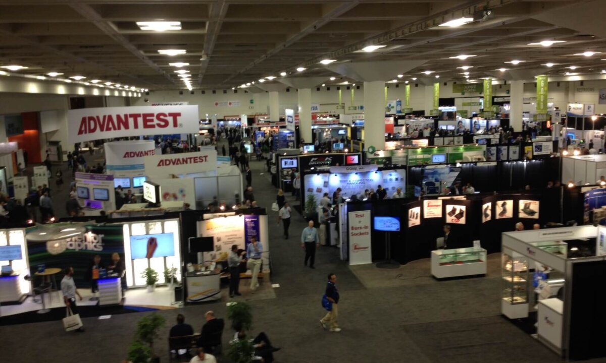
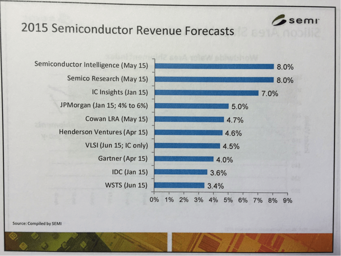
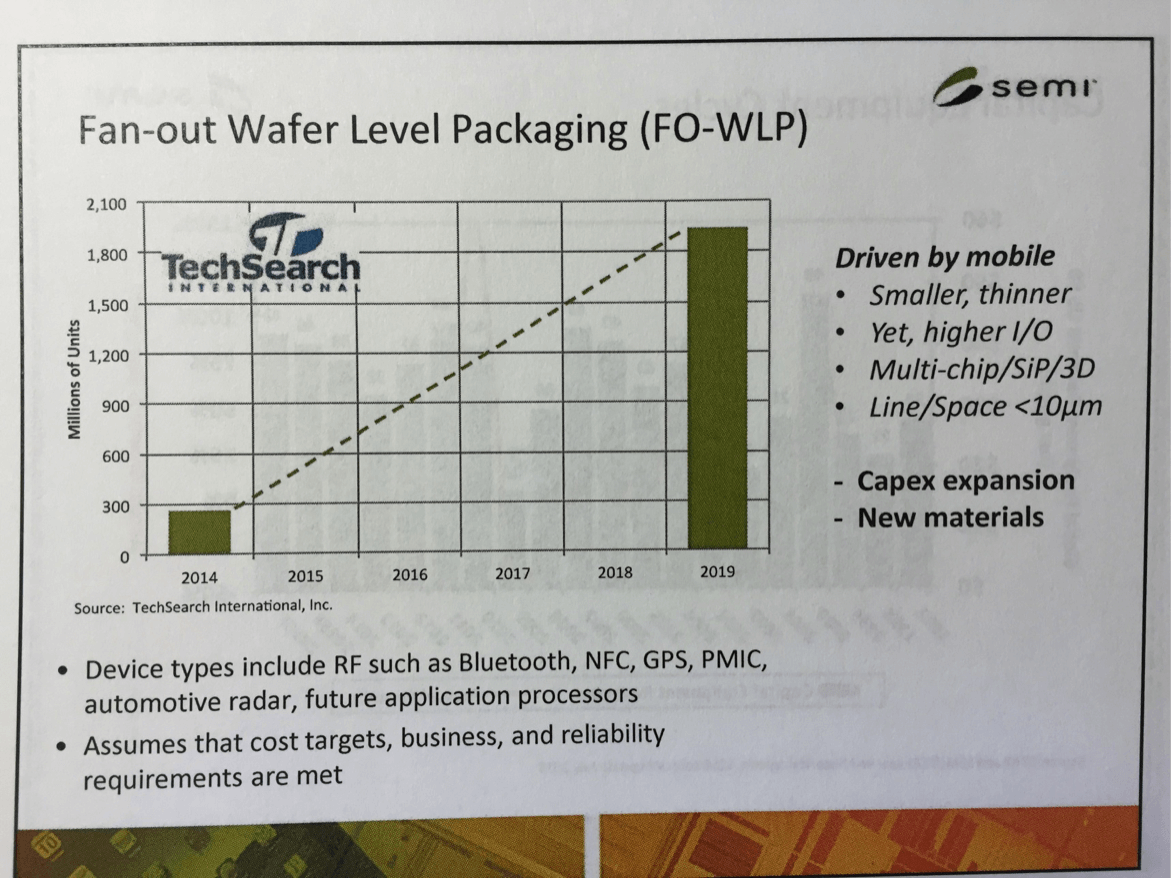
After Karen Savala, president SEMI Americas, welcomed us to the 45th SEMICON Conference, Dan Tracy, SEMI’s senior director of Industry Research & Statistics – Market Forecast, told us that SEMI expected 26,000 visitors for SEMICON 2015. He reported that 692 companies were exhibiting this year, an impressive 136 of them were new exhibitors. Dan also showed the broad range of semiconductor revenue forecasts (slide 1) and a very promising forecast from the typically conservative TechSearch International team for wafer-level packaging (slide 2).

Tuesday’s keynote panel: “Scaling the Walls of 14nm Manufacturing” was very informative. With imec’s Jo de Boeck as moderator, Qualcomm’s Mike Campell, ASE’s Calvin Cheung, Stanford’s Subhasish Mitra and Globalfoundries’ Gary Patton contributing, a very interesting and frank discussion developed. They mentioned that following Moore’s Law doesn’t offer the same level of improvements any more, emphasized that die AND package yield are key, talked about variability becoming a bigger design- as well as manufacturing challenge with smaller feature sizes, reminded us that the software content – and with it, the memory content – of systems in increasing, talked about the currently underestimated die-package interaction and assembly challenges and demanded, like other speakers at SEMICON, closer cooperation across the supply chain, specifically between assembly houses and IC design teams.
Intel’s Doug Davis presented Wednesday’s keynote: “The Internet of Things and the next fifty years of Moore’s Law”. A short movie looked back at the tremendous progress continued shrinking has enabled. Then Davis focused on the impact IoT edge nodes and data centers’ compute capabilities will contribute to making our lives better. With demos and examples, Davis illustrated the impact this technology will have on 1) elder care, 2) the environment, 3) the urbanization boom and 4) agriculture. He substantiated the need for sensors and compute power in all four segments with market research data, short demos, and very plausible analytics. Like many previous speakers, Davis also called for industry-wide cooperation and the need for standards. He mentioned the Industrial Internet Consortium and the Open Internet Consortium as examples for cooperation and standards development.
When walking the exhibition floor and talking with people, I learned that equipment vendors are nervous about the ongoing industry consolidation and the price pressure they get from wafer foundries. At the same time they see significantly increasing interest in their equipment from assembly houses. A clear sign that these assembly houses are investing in the middle-end-of-line (MEOL) (Wafer thinning and handling, TSV last insertion, backside processing with RDLs, bumping, etc.). is an important sign of more value creating shifting towards the so-called OSATs. Let’s hope next year’s DAC and SEMICON will address this important shift of paradigm in much greater depth than this time. ~ Herb