


I’ve been following the Alchimer story as it unfolds ever since I first started following the course of 3D integration in 2009. In my opinion, the technology has been cool and disruptive pretty much since day one. The wet, electrochemical process that enables growth of nanometric films offers an elegant, high yield alternative to traditional deposition processes for metallization. However, finding the right toehold in the industry has been a bit of a challenge, as the company tried out different business models and went through a number of management reorganizations.
This week at SEMICON West, Alchimer adds a new chapter to the story: it’s got a new name with a new focus and new business model, and is ready to take its technology to the next level, out of the lab and into production. In this executive viewpoint interview, 3D InCites speaks with Bruno Morel, CEO, aveni, about the transformation from Alchimer to aveni and how it will enable the future of 3D ICs.
Why aveni?
Alchimer is known as an R&D focused company. Its purpose is to develop and fine-tune the all-wet nano-scale metallization processes and chemistries for dual damascene and 3D TSV applications. The business model has evolved from licensed to royalty-based. According to Morel, recent developments in technology readiness, industry partnerships, and funding (13.5M from various sources) positions the company for a bright future, and warrants a rebrand and reorganization. “aveni is derived from ‘avenir’ (French for ‘future”) and demonstrates forward thinking and vision,” said Morel. “We now have materials and processes ready for production. It’s time to move forward with a new name. aveni represents that.” Morel said Alchimer’s executive team is transferring to aveni, and the product lines, eG (electrografting) and cG (chemical grafting) will remain the same as they move from R&D to manufacturing.
aveni’s business model will be neither royalty nor IP license based, but will follow a more traditional path, selling chemical formulations and providing process support and set-up over the life of the product, said Morel. Morel says the company is working with equipment vendors to integrate eG and cG processes into traditional deposition tools.
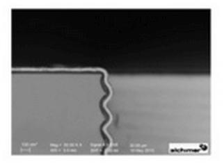
Figure 1: SEM of isolation/barrier/seed on a scalloped TSV. (courtesy of aveni)
Part of the ongoing story has been that these all-wet growth processes (vs. vapor phase deposition processes) for metallization provides 100% conformal step coverage over whatever topography it faces; for Through Silicon Vias (TSVs) this translates to isolation/barrier/seed/fill steps at a lower cost, with the ability to metallize 10:1 aspect ratio TSVs and below (Figure 1). Up until now, these capabilities alone haven’t inspired manufacturers to implement the processes into the 3D IC process flows, despite the fact that they don’t require tool adaptations and offer customers greater value. I asked Morel, what has changed? Why now?
Morel explained that a number of things have changed to create a perfect storm. First of all, as Alchimer, they were working with R&D labs and customers to establish proof of concept. As aveni, they are partnering with equipment companies and semiconductor manufacturers at the manufacturing stage who are looking at metallization solutions for the worldwide market.
Second, the needs of the market are changing, and we are reaching the capability limits of traditional metallization processes like PVD and ECD, in meeting those needs. At 5:1 aspect ratio, many processes work. At 10:1 and higher, that isn’t the case, noted Morel. “When something works, you try to squeeze as much as you can out of it to get better value and yields,” he explained. “We have reached a point in time where the industry requires high aspect ratio TSVs, and can’t accept average yields. Older technology can no longer sustain those requests.”

Timing is Everything
With product roll-outs integrating 3D DRAM in high-end graphics applications, and a push towards technology optimization to lower costs to bring 3D ICs into mainstream consumer applications, the timing for aveni couldn’t be better. Atomic layer deposition (ALD) has been the traditional approach for metallizing HAR vias and it’s very expensive. “One year from now, we won’t be talking about a roadmap; aveni technology will be a fact. For high aspect ratio vias, customers will have to choose between ALD and aveni’s technology. We can provide a solution today. As a result, customers are much more open to the conversation.”
And so aveni takes the eG/cG story into its next chapter. I look forward to see what comes next. ~ F.v.T.
aveni’s process will be mentioned later this week at SEMICON West, during the session, What’s Next for MEMS? Claude Jean, of Teledyne Dalsa Semiconductor will be presenting some case studies on technology innovation in his talk titled, Challenges for MEMS Foundries in a Highly Captive MEMS Market.


