


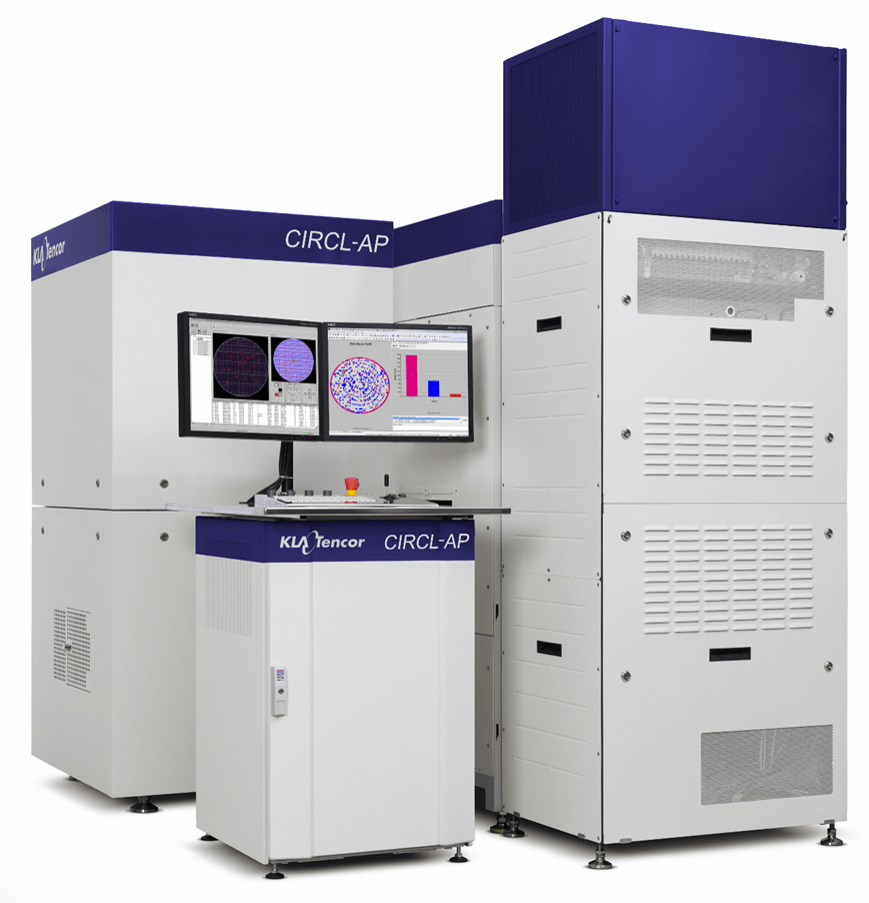
 CIRCL-AP™ is a cluster tool with multiple modules, covering all-surface inspection, metrology and review at high throughput for efficient advanced wafer level packaging (AWLP) process control. The CIRCL-AP provides production-proven, high sensitivity monitoring capability for multiple AWLP applications including 2.5D/3D integration, wafer-level chip scale packaging and fan-out wafer-level packaging.
Testimonial
CIRCL-AP provides differentiated process control to the expanding field of 2.5D/3D manufacturing, helping optimize packaging processes for development of Cu-pillars, bumps, TSVs and redistribution layers (RDL). CIRCL-AP is currently being used for the ramp of 3D memory stacking for high performance applications, while ongoing collaboration with OSATs is driving improved yield for next-generation WLCSP and fan-out process flows. With a modular configuration, the CIRCL-AP has been adapted to support a wide range of AWLP processes. The 8-Series front side defect inspection and metrology module captures critical defects (e.g. TSV cracks, RDL shorts, deformed or missing bumps and Cu pillars) and provides 2D metrology for RDL, bumps and TSVs. The CV350i edge inspection, profile and metrology module has proven critical for successful implementation of temporary bonding processes—enabling detection of edge trim issues, excessive glue squeeze-out, edge voids and other defects. Finally, the Micro300 module provides X, Y and height metrology for monitoring multiple AWLP applications, including TSV reveal process, RDL line space, micro-bumps and Cu pillars.
KLA-Tencor Website
Date this Product was Introduced to the market: April 2015
Category Product is Being Nominated for: Inspection/Metrology Tools
Technical Documentation for the Circl-AP™


