As promised in part 1 of my ECTC 2015 blog about this impressive conference, see below summaries of presentations I found very useful to contribute to the advancement of single- and multi-die packaging. To make it easier for the reader to dig deeper and review the entire paper, I included in every summary the paper number, as listed in the program and on the USB stick we received.
As I mention in part one, my single-core, single-threaded mind and body allowed me to only attend one presentation at a time. Most of the time I chose “Advanced Packaging”, from the six tracks offered. Therefore most of this blog will cover this particular subject.
Wednesday morning started out with a presentation from Amkor (s01p1), describing how they assure reliability in high-performance flip-chip devices for mobile and IoT applications, in spite of needing the brittle ultra low-k dielectric material. The presenter described the assembly steps and temperature profiles used to minimize stress due to CTE differences between chip and package.
The following Qualcomm presentation (s01p2) focused on a closely related subject: Thermal compression flip chip (TCFC) bonding of fine-pitch copper pillars with solder tips. The paper outlined a 15x15mm test chip with an 11x11mm die using 80μm bump pitch with room for one escape route in between. The speaker also presented reliability test results and cross-sections to demonstrate HVM readiness of this technology.
Another paper (s01p5) I found very useful was from the equipment supplier, Kulicke and Soffa. Bob Chylak showed the throughput, cost comparisons, as well as trade-offs for different thermocompression processes. He conveyed that flip chip packaging technology, an important building block for multi-die packaging, is getting more and more cost effective, as equipment- and materials vendors work closely with their customers to develop HVM solutions.
Wednesday afternoon started with a presentation from Xilinx (s07p1). They invested several years in the development of the Virtex 7 2000T quad FPGA and were the first company introducing an interposer-based 28 nm multi-die IC, in late 2010. They expanded the product family and production volumes since. Bahare Banijamali presented some technical details about the latest generation of this leading edge design: This IC combines three 20nm FPGA slices, 14x23mm, with 375,000 micro-bumps each. The 100μm thin interposer is 25x45mm large, uses 10μm copper TSVs and 30,000 bumps, spaced at 40μm, to connect with the 55x55mm organic substrate. Banijamali pointed out the different TCEs of the materials deployed and showed how Xilinx assures exhaustive testability. He also demonstrated that the parts passed component level TC and HTS. In addition, Xilinx mounted four such devices with C4 bumps, side-by-side, on a 3.42mm thick PCB for reliability testing. They saw the first failure after 1645 cycles. Banijamali explained the failure mechanism and projected, based on further reliability testing, a characteristic life of 2275 cycles. This extremely demanding application demonstrates quality and reliability of TSMC’s CoWoS technology as well as assembly know-how of Xilinx’ partners.
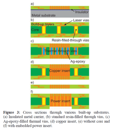
The paper S07p5 described a cooperation between GeorgiaTech, Mitsubishi and Ushio. They studied fundamental factors that impact the scalability of organic interposers. As silicon interposers are costly and limited to lower frequencies (due to high insertion loss) fine-pitch organic interposers become more attractive. The team modeled, designed, and manufactured a test vehicle with two 10x10mm die on a 2-2-2 organic interposer, 19x24mm large, with only 100μm thickness and 40μm pitch. They also designed and fabricated an RDL test vehicle, without the power/GND planes in the core of the organic interposer. The presenter outlined simulation / test results and even recommended design rules for designers of fine-pitch organic interposers.
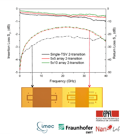
each transition allows to
decrease considerably
the insertion loss.
• Characterization
performed for arrays up
to 5×10 TSV per
transition. (source, Fraunhofer EMFT)
On Thursday morning, in addition to several calls and 1-on-1 meetings, I managed to listen to paper s13p7. It covered how tungsten-filled TSVs in high-resistivity silicon (4.5kOhm.com) serve RF MEMS applications. This work originated out of the E-BRAINS project. EPFL, Fraunhofer and IMEC showed the innovations my European friends are driving for design and manufacturing of wave guides, TSVs, and MEMS for RF applications. The presenter outlined integration challenges and process flows, explained the reasons for low temperature profiles, showed cross sections, characterization and reliability test results (Figure 1).
In the afternoon I found paper s19p4 from GeorgiaTech useful for very high power-density designs. Li Zheng, a Ph.D. candidate, presented a silicon interposer design with embedded microfluidic cooling they developed for a high-performance computing systems (Figure 2).
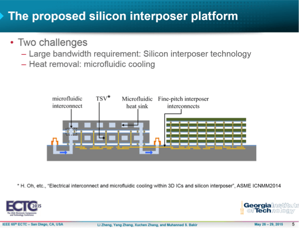
While interposers, compared to 3D vertical stacking, offer much better opportunities for air-cooling, this liquid-cooling concept takes this benefit a significant step further. The slide above shows how the Georgia Tech team combined a memory cube and liquid-cooled logic dies on an interposer.

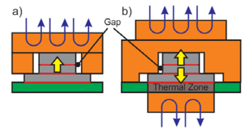
Paper s19p5, presented by IBM’s Thomas Brunschwiler, outlined another way to cool, specifically vertically stacked, dies. IBM showed how a) single-sided, as well as b) double-sided cooling of a die stack keeps temperature under control and assures reliability.
Brunschwiler also discussed the significant impact thermal vias can have in managing die temperatures.
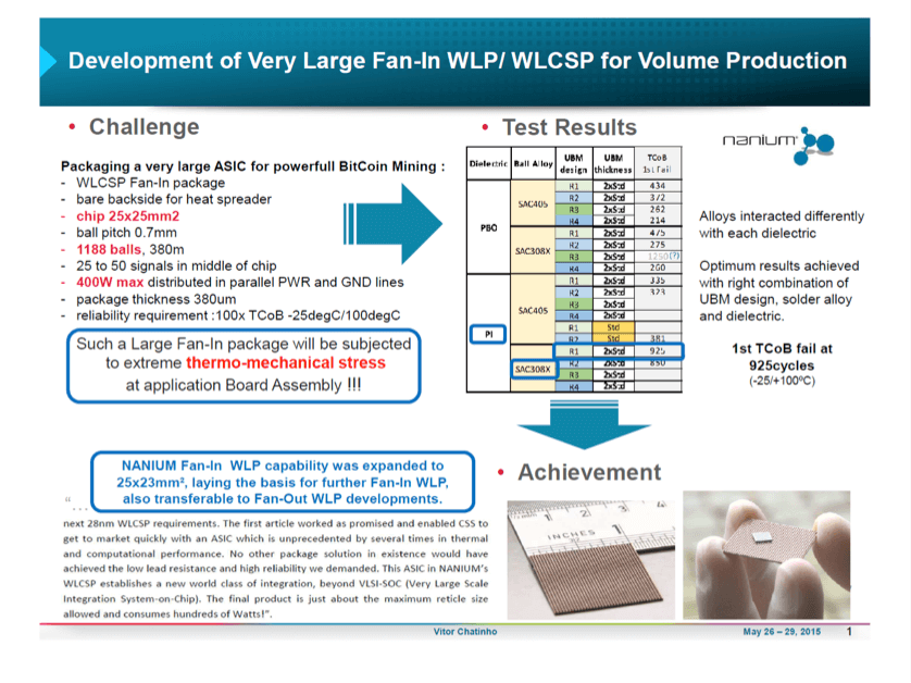
On Friday morning, a presentation from Nanium S.A. drew my attention. Their expertise is wafer-level packaging. Vitor Chatinho presented with paper s25p5 how they managed to ready a very large Fan-In WLP design for volume production. The slide below summarizes key points mentioned by the speaker.
Soft copies of all papers were given to attendees of this conference for further studies. If you were not able to attend, check with the conference organizers or IEEE to find out if and where you can download all papers, including the ones referenced above. ~ Herb