


While we wait in the 3D IC holding pattern for products to go into high volume, processes continue to be tweaked and optimized to address the remaining 3D IC assembly challenges. At IMAPS DPC 2015, a number of presentations focused on some of these incremental advancements. Here, we checked in with several processes that we’ve been following closely as they have evolved over the past few years, and past few months.
According to Jeff Calvert, Dow Electronic Materials, it may have not looked like new information based on the abstracts and the titles, but the presentations the company gave on temporary bond/debond materials as well as TSV fill demonstrated that there are still improvements being made.
In the TSV fill realm, Dow’s Matthew Thorseth presented results using Dow’s latest Cu TSV plating bath in an Applied Materials plating system. By developing and selecting the proper organic additives, optimizing the plating process, and implementing advanced bath control techniques that enable short TSV electroplating times, they filled 10×100μm vias in less than 1 hour and 5×50µm vias in under 20 minutes. According to Thorseth, this combination also exhibits low overburden for stress management, CMP cost reductions, and high reliability.
Dow first introduced its BCB-based temporary wafer bond (TWB) material at IMAPS DPC in 2013. In that presentation, they demonstrated the mechanical debond capabilities. In David Fleming’s presentation at IMAPS DPC 2015, he also demonstrated the material’s success for a laser debond process. He offered two scenarios using the most prevalent laser sources – 248nm and 308nm – to successfully debond the active wafer from the carrier cleanly, leaving only a TWB film on the device wafer that can easily be tape-peeled off.
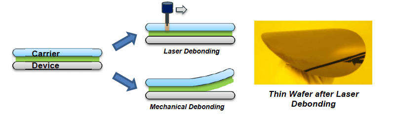
With the 248nm laser source, no modifications were needed. With the 308nm laser, modifications were necessary. Dow produced a thin, laser-active region between the carrier and the TWB that acts both as an adhesion promoter and ablation layer that can absorb 308nm laser light. This allowed for successful debond, leaving the same, easily removable tape-peeled film on the device wafer.
In general, it’s believed that TSV fabrication and backside processes are well in hand interposer integration and 3D ICs, but according to Guilian Gao, Invensas, challenges still remain in backside processing and assembly largely because of the low backside processing temperature imposed by the poor temperature stability of the temporary bonding adhesive and other organic materials; the complicated logistics of the FAB-OSAT-FAB transportation; and the reduced feature sizes of micro-bumps in combination with very large, thin interposers.

Invensas has been addressing these challenges for some time, and in the last three presentations I’ve attended at three separate conferences, have focused on three selected process flows — two using chip-to-chip assembly and one chip-to-wafer—on two Si interposer test vehicles, and reporting findings for different critical steps in the flows. One test vehicle used a rectangular silicon interposer of 19x27x0.1mm and was put through an assembly-centric chip-to-chip process flow (Figure 2a). The other used a square silicon interposer of 24x24x0.05mm and was put through a fab-centric, chip-to-wafer process flow (Figure 2b). At IMAPS International 2014 in September, Liang (Frank) Wang, Invensas presented a solution to the temporary bond/debond issue by replacing the temporary carrier with a permanent one, which also prevents warpage and provides good planarity.

In November 2014 at the International Wafer Level Packaging Conference (IWLPC 2014) Guilian Gao presented an in-depth analysis of interposer and 3D IC assembly process window and guidance on how to select the right assembly flow to preserve the µbump interconnect. According to Gao, the greatest challenge facing interposer integration and 3D IC assembly is the shrinking assembly window – literally how much space you have to perform assembly processes. Unlike flip chip assembly, in which you had to work with the volume of a full solder ball with much larger diameter, microbumps are much smaller in diameter and the solder on the tip of the Cu pillar is only a half-ball. “When you have a 3-4x reduction in pitch, the assembly window goes down 10x.” explained Gao. Therefore controlling warpage and microbump height variation becomes very critical for assembly yield. She also focused on subsequent processes of flux cleaning, underfill and molding.
Most recently, in her IMAPS DPC 2015 presentation, Gao used the 2 test vehicles to demonstrate the pros and cons of chip-to-chip and chip-to-wafer assembly processes. Gao’s work with the test vehicles in two of the three process flows addressed the warpage control and microbump height variation. Flow one (chip-to-chip with thin interposer to package substrate attachment first) was used to demonstrate how bad the warpage would be when the interposer was first attached to the package substrate, and then the microbump dies were attached using SnAg Cu pillars.
In the improved assembly-centric flow 2, the microbump dies were attached to the thinned interposer first using SnAg Cu pillars, then to the package substrate. Since you’re now soldering silicon to silicon with no CTE mismatch at this stage, the warpage can be contained, explained Gao. One complication with this flow is that the flip chip solder bumps cannot be put on the thin interposer before the microbump die assembly. After the microbump die to interposer assembly, the flip chip solder bumps can be formed on the interposer backside or on the package substrate. Invensas chose to put bumps on the substrate rather than the interposer, which has bump pads. The logistics of this flow is simpler because the fabrication of interposer precedes the assembly process.
In the fab-centric, chip-to-wafer flow, direct Cu-to-Cu bonding was used to form the interconnect between the thinned die and the interposer wafer instead of soldering. The stack was then bonded to a permanent Si handle wafer. There is no temporary bond/debond involved. The interposer was thinned to 50µm and attached, to the package substrate. With this process flow, there are no warpage issues. However, the logistics is more complicated because of the interweaving processes of interposer fabrication and assembly, unless some of the traditional assembly processes find their way into the fab.
The work discussed here being done at both Dow and Invensas exemplifies the efforts across the supply chain that are ongoing to further improve and optimize interposer and 3D IC processes to improve yield and lower costs in an effort to bring us closed to high volume manufacturing. ~ F.v.T.


