
Continuing from Part 1:
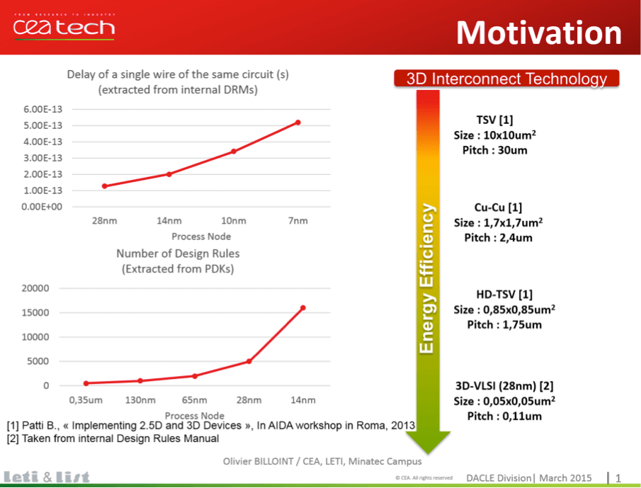
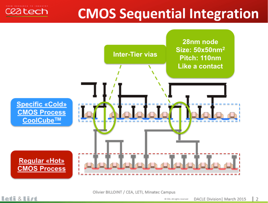
On Thursday morning I really enjoyed the Monolithic 3D session. Francoise already reported about it, so I can be brief and focus on the most advanced program presented, the CEA Leti CoolCube™ . Olivier Billoint showed and explained how Leti, in cooperation with an EDA partner, is developing the integration of two layers of functions on a wafer. The first layer uses a regular “hot” processing technology for all steps in the wafer fab. For the second processing run, Leti developed a “cool” processing technology, to not degrade the devices manufactured during the first processing run. In addition to these key processing recipes, Olivier outlined some specific material needs as well as the special EDA support for place and route, clock distribution and other design flow changes needed. Slides 1 and 2 below outline the motivation for developing this technology, as well as show the stunningly small geometries – compared to stacking individual dice – this technology can achieve. EPFL Lausanne and Stanford University also presented their research efforts in 3D Monolithic technology and are covered by Francoise.
 On Friday, DATE offered 10 different workshops, focusing on these important topics: Abstraction and Modeling, EV Battery Packs, Neuromorphic Computing, Hardware Design, 3D Integration, Multicore Architectures, Designing with Uncertainty, Embedded Image Systems, Optical/Photonics Interconnects and Secure Devices. Because of my focus on multi-die designs, I of course attended the workshop titled: 3D Integration Technology, Architecture, Design, Package, Automation and Test. It was chaired by Saqib Khursheed from the University of Liverpool and Pascal Vivet from CEA-Leti.
After the welcome address by Pascal, Paul Franzon from NCSU presented the keynote and demonstrated in many different ways how interposers and vertical die-stacking increases performance, while reducing power dissipation and form-factor, compared to our traditional ways of implementing computing– and networking equipment.
Tezzaron’s Bob Patti explained how different levels of cache memory are getting implemented today and showed how embedded memory increases CPU/GPU die-sizes significantly while external memory cause cache misses, due to long and very power-hungry interconnects, and limits CPU/GPU performance significantly. Bob explained Tezzaron’s DiRAM architecture and benefits, then discussed how photonics interconnects can help reduce access times for CPUs to far memories, where the delays electrical ←→ optical translators introduce can be justified.
Following Bob’s high-performance computing focus, Andreas Hansson from ARM gave us a low-power perspective. He outlined ARM cores and architectures, then compared the performance/power ratio of today’s popular DIMMs with multi-die packaging. The later clearly complement ARM’s commitment to lowest power solutions.
After a short coffee break everybody was charged for Francoise’s part of the workshop. First Krishnendu Chakrabarty from Duke University talked about the progress probe-card vendors have made to improve wafer probing and the probability for achieving known-good dice (KGD). Formfactor as well as Cascade Microtech, in cooperation with IMEC, have developed reliable solutions for probing tightly spaced points. Then he explained why pre-bond, mid-bond and post-bond test-steps should be introduced, when die-yields and stack complexity justify these steps economically. Krishnendu also talked about the ongoing P 1838 test standardization efforts and the resulting benefits for the 3D-IC ecosystem.
Then the most interactive part of the workshop started: Francoise’ panel discussion titled,
“Will 3D integration break down memory bandwidth barriers? How and when?” Panalists were:
- Geert Van der Plas from IMEC
- Denis Dutois from Leti
- Mustafa Badaroglu from Qualcomm
- Hsien-Hsin S.Lee from TSMC
- Brendan Farley from Xilinx
To assure a very active discussion, Francoise had prepared 15 agree/disagree statements and used Kahoot to capture the audience’ position on her points. Panelists and audience quickly addressed the panel’s title and concluded that 3D integration will break down the dreaded memory wall. Both sides even mentioned examples for designs that are already enjoying the much higher bandwidth interposers and vertical die stacks enable.

Kahoot enabled Francoise to display the audience’ response on every one of her 15 statements. Based on the results, the panel chose to table points where participants were in agreement, and steered the discussion to the points where the audience was divided. In the ensuing discussions both sides explained their positions and typically very quickly clarified why they took a particular position. These constructive dialogs surfaced a lot of good information, e.g.:
- Memory cubes from Hynix, Micron and Samsung, mounted side-by-side with CPUs, GPUs or other logic chips on interposers offer significant performance versus power benefits and are already in many design projects.
- Except for memories, TSV-interconnected vertically stacked die are rare at this time – primarily due to lack of trust-worthy design tools.
- Silicon interposers are too costly to only provide a few interconnect layers; suppliers and users are working on adding passive functions (R, L, C), some even look further and develop interposers with power management circuits, ESD structures, MEMS and other active functions.
- Placing one or several silicon interposers, together with logic, analog, RF or other dice on a large organic interposer, offers both very high density routing and lower unit cost.
- TSV-less interposers, and interposers replacing the package substrate also help reduce cost.
- Wafer-level packaging is seen as a very effective way to significantly reduce unit cost.
After lunch, Robert Fischbach from Fraunhofer in Dresden presented their work on die-package-board co-design and demonstrated the benefits of both the package- and PCB impact on the silicon design. Floorplanning, pin-assignment, power integrity, signal integrity, thermal and thermo-mechanical considerations are needed to result in a cost-effective and reliable IC design.
My presentation was next and focused on improving cooperation and dataflow between IC assembly houses and IC designers and their captive packaging experts. I suggested to work with assembly houses and their material suppliers to model package and substrate capabilities accurately. We should capture this data in an “Assembly Design Kit” (ADK), in XML format and transmit it, in encrypted form, to the IC designers’ EDA tools. Just like “Process Design Kits” (PDKs) enabled very efficient cooperation between wafer foundries and the fabless IC vendors, ADKs will streamline the customers’ cooperation with assembly houses. The following Q&A session raised topics like:
- A universal design kit (UDK) – combining PDK and ADK – may be even better.
- The assembly houses have very thin margins and may not be able to finance the required efforts. Who can fund it?
- Several ideas regarding what else such an ADK should contain were discussed as well.
Georg Kimmich from STMicroelectronics is well known for driving, together with Leti’s Denis Dutoit, the Wioming test chip development at STEricsson, a few years ago. Georg endorsed my ADK proposal as a good first step, but, based on his vast experience in 3D technology, reached a big step further and suggested to target a Universal Design Kit, combining PDK and ADK to empower IC designers even more. He suggested to target as the first step DRC sign-off, then DRC-aware design and finally yield-aware design, spanning across silicon, package and PCB considerations. He also noted that many of today’s EDA tools still can’t digest the complexity of multi-die designs and recommended to establish strict rules to avoid surprises.
The last presentation I was able to attend, before starting my return trip to California, was from John Ferguson, the marketing director in Mentor’s Calibre Group. John described Mentor’s current 3D capable tools, emphasized Mentor’s commitment to expand the current range of available tools and the current die-package-board design flow. He showed a roadmap to a broad range of 3D tools and explained why all parties in the 3D Ecosystem need to work together to develop tools and methodologies for multi-die designs. To minimize risk and design times, Mentor will offer reference flows as well as educate and train users on how to best utilize all these capabilities to develop sub-systems, even entire systems with interposer and 3D-IC designs.
The day concluded with a final session that focused on test and technology challenges for 3D IC, chaired by Makoto Nagata, of Kobe University, as well as a poster session. If you were unable to attend this workshop, be sure to put the D43D Workshop on your calendar. It takes place June 22-23, 2015, in Grenoble. ~ Herb