
Emerging “More than Moore” and photonic applications benefit tremendously from the close integration of compound semiconductor materials. Recently, many of the improvements in device performance achieved within the semiconductor industry are a result of innovation and material research rather than traditional downscaling of design features. One of the major new trends in semiconductor materials-based innovation is combining the benefits of mature Si technology and the superior properties of III-V materials. This is gaining a lot of attention these days due to the high electron mobility and optimal optical properties of integrating Si and III-V materials, which enables high-performance transistors and silicon photonics, respectively. Nonetheless, the need for heterogeneous integration of compound semiconductor materials is not limited to CMOS wafers and can be extended to economical substrates in general.
Wafer bonding is a key technology for several developed heterogeneous integration schemes as it allows one to directly combine different material without degrading the crystal structure. It has already been proven for several years that plasma-activated fusion bonding is a reliable method for producing engineered substrates. In fact, activating the substrate surface with plasma treatment is the key to making direct wafer bonding accessible for compound semiconductors since it enables the joining of different materials at room temperature. Traditional annealing processes developed for SOI wafer manufacturing required an annealing temperature of 900°C as the oxide interface had to get into a state of viscous flow. This is far too high for materials with different thermal expansion coefficients as the introduced stress results in large wafer bow or warpage and can lead to cracking of the wafers. In contrast, fusion wafer bonding is a low-temperature plasma activated direct bonding process based on oxidation within the interface as described in further detail by Plach et al.¹ The surface activation lowers the required annealing temperatures significantly below 400°C while still providing high bond strength. As a consequence, the critical stress is not reached for most material combinations and almost any compound materials can be integrated on alternative substrates.
The same technique can be used to co-integrate III-V and Ge CMOS to create new hybrid CMOS circuits. As III-V materials are best for electron transport and SiGe-MOSFET is preferable for holes, new circuit architectures that combine both types of transistors demonstrate high performance at low power as desired for mobile applications. Direct wafer bonding has been demonstrated to be the preferred method to achieve this, since epitaxial growth has shown strong limitations for co-integration.
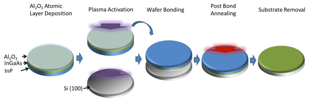
Often CMOS temperature restrictions to 400°C are exceeded by several hundred degrees during epitaxy of compound semiconductors. The image below shows the process flow typically used to enable these promising devices, using plasma activated direct wafer bonding as replacement to hetero-epitaxy.
Scaling to 300mm wafers is key to enabling volume production of heterogeneously integrated compound semiconductor devices. This could be facilitated by breaking the given geometry constraints of bonding full wafers. Wafer-level die transfer processes preserve the main advantages of wafer-to-wafer bonding.
In this case, the compound wafer is reconstituted to an intermediate carrier. This allows collective pre-processing and plasma activation of the dies. On the other hand, this enables a high die bonding throughput on wafer level. This cannot be provided easily with die to wafer fusion bonding. Wafer-level die transfer processes combine the best of two worlds, which is the fast distribution of known good die, and high-quality direct bonding.
However, plasma activated fusion bonding is not suitable for devices relying on vertical current flow, where an electrically conductive interface with optimized ohmic behavior might be crucial. Prominent examples of this are multi-junction solar cells and vertical power devices. Recent developments, such as EVG’s ComBond® technology, can provide a covalent oxide-free bond interface that addresses these needs. Furthermore, this new approach allows one to join different materials at very low or room temperature, thereby keeping the internal stress between the wafers at a minimum.
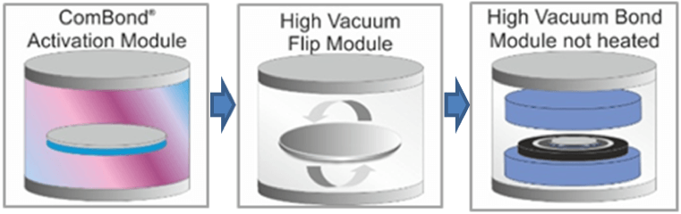
EVG’s ComBond technology enables the removal of the undesired oxide layer with a dry process utilizing energized particles. Unlike the fusion bonding process where nanogaps are closed through oxidation, the ComBond process is best described on the atomic scale. The surface treatment results in dangling bonds on the wafer’s surface, which is required for a room-temperature covalent bond. The CAM module (ComBond Activation Module) on the ComBond system enables effective oxide removal while simultaneously minimizing damage of the underlying substrate material, which is essential to a successful bonding process as described in further detail by Flötgen et al.²


Keeping the wafers in a high-vacuum environment after surface removal prevents re-oxidization of the semiconductor surface while the wafer is undergoing further processing in the bonding cluster system. Since the surface preparation step takes only a few minutes for each wafer, re-oxidation can be prevented for several substrates and activation conditions.
In summary, direct wafer bonding has evolved in recent years from primarily being used in the manufacture of SOI wafers to becoming a production proven process for heterogeneous integration of compound semiconductors. The latest advances in direct wafer bonding demonstrated by the ComBond process even overcome restrictions that other fabrication methods face, such as scaling of compound materials to larger substrates or joining different materials with an oxide free interface. In particular, the ComBond process with its minimum impact on the crystal structure and ability to provide electrical conductivity via the interface can be key-enabling for several applications. Overall, wafer bonding for heterogeneous integration can pave the way for innovative device designs with novel functionalities and increased performance.
References
[1] T. Plach, et al., J. Appl. Phys., 113, 094905, 2013
[2] Flötgen et al., ECS Transactions, 64 (5), 2014
Author Bios
 Dr. Thomas Uhrmann is director of business development at EV Group (EVG) where he is responsible for overseeing all aspects of EVG’s worldwide business development. Specifically, he is focused on 3D integration, MEMS, Compound Semiconductor and a number of emerging markets. Prior to this role, Thomas was business development manager for 3D and Advanced Packaging as well as Compound Semiconductors and Si-based Power Devices at EV Group. He holds an engineering degree in mechatronics from the University of Applied Sciences in Regensburg and a PhD in semiconductor physics from Vienna University of Technology.
 Dr. Martin Eibelhuber is business development manager at EV Group for bonding, lithography and nanofabrication technologies and particularly focusing on compound semiconductors.
He holds a PhD in technical physics from the Johannes Kepler University Linz specialized on nanoscience and semiconductor physics. As a university staff member he gained professional experience in photonics, nanofabrication, and material characterization.