


Ever since 3D transistors (aka FinFETS or Intel’s Tri Gate) 3D NAND, and monolithic 3D IC processes joined the family of 3D integration technology possibilities, we’ve been careful to define them separately on 3D InCites. Some people have wondered if one will displace the other, or if these technologies would delay the adoption of 3D stacked ICs using TSVs. I maintain that these technologies have different applications, and while advancements in existing advanced packaging technologies have certainly delayed adoption of 3D IC stacks at the package level, 3D transistors and 3D NAND have not had the same impact. Moreover, in my opinion, theoretically, these are complementary technologies that could, in fact, be stacked on an interposer to create a device that I like to call “3D on steroids”.
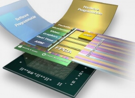
This week’s introduction of Xilinx UltraScale+ family of FPGAs, confirms my theory. According to the company, the devices integrate 16nm finFET vertical 3D transistors on an interposer (that’s the 3D-on-3D part); along with enhanced memory; and multi-processing SoCs (MPSoCs), which integrate “the right engines for the right tasks” including “soft and hard engines for real time control, graphics and video processing, waveform and packet processing, and multi-level security, safety and reliability, and more”. The company claims that these devices achieve “5X greater system-level performance/watt over 28nm devices, far more systems integration and intelligence, and the highest level of security and safety.” The integration is interposer-based, and implements the company’s new ‘SmartConnect’ technology, which reportedly ‘applies interconnect topology optimizations to match design-specific throughput and latency requirements while reducing interconnect logic area.” Julien Heppich, EETimes Europe, wrote a detailed description of the technology here. (The Xilinx website also has tons of technical information available for the really curious.)
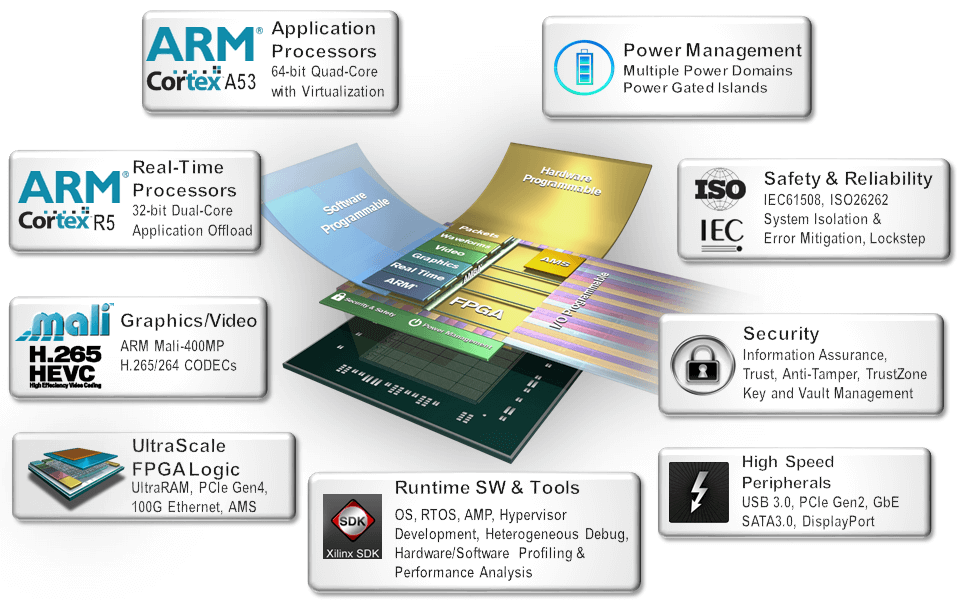
The new product family is currently undergoing customer evaluations, with tape-out expected in Q2 2015, with first shipment to customers by Q4. Target applications are as expected, high computing applications, next-generation wireless, and industrial Internet of Things (IoT). The added security element is likely what makes it so appealing to IoT applications, as that is of significant concern. Achieving this milestone involved collaborative efforts with ARM, TSMC, and Xilinx’ design service alliance members (DornerWorks, DornerWorks, Fidus Systems, Green Hills, Lauterbach, Lynx Software Technologies, MathWorks, Mentor Graphics, Micrium, NI, Northwest Logic, TED Inrevium,, Topic Embedded Products, Wind River, and Xylon)

There are a number of really cool things about this announcement. First, it’s the first product that uses 3D transistors stacked on an interposer, taking 3D to a new level (no pun intended). Second, it further strengthens the argument that interposers are an enabling technology, and not the bridge to “true 3D” that they were first thought to be. Third, this appears to be the first product realization of what we’ve talked about at length over the past year: partitioning SoC designs into functional blocks and stacking them on an interposer for improved power and performance at a lower cost than planar scaling. It looks like Xilinx has done it again! ~ F.v.T.


