


The distinguished journalist Peter Clarke, writing in EETimes on 02 January 2015, identified what he called the “15-in-15: Analog, MEMS and sensor start-ups to watch in 2015.”
What better place to shine the heterogeneous integration spotlight than here, I thought, when I read the piece in January – as Peter wrote, “The blossoming of the [Analog, MEMS, Sensor] sector may be to do with the general buoyancy of the total global semiconductor market, … and to the fact that analog, MEMS and sensor activities seem to be doing slightly better than the overall average. … There is not only scope for a greater number of more sophisticated sensors in [mobile handsets] but also for the same or similar sensors to appear broadly across other equipment from automotive to industrial and medical.”
What would we find, I thought to myself, were we to look for heterointegration spoor amongst these 15 notable start-ups?
Examining in turn the first five companies from Peter’s list I found this:
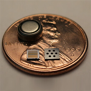
Cambridge CMOS Sensors: CCS is active in the semiconductor and gas sensor community, and say they are the industry leader in advanced sensor solutions and sensor technology for monitoring indoor air quality (IAQ), including VOCs and hazardous gases (such as CO), outdoor air pollution levels, and breath analysis across multiple global markets. CCS is a fabless semiconductor company; the sensors themselves, essentially micro-hotplates, are fabricated on a standard CMOS MEMS process and are shipped in a compact 0.99mm x 2.0 x 3.0mm SMD package that is said to be suitable for high-volume consumer applications.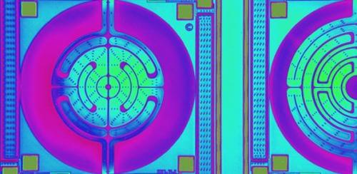
The CCS family of MOX gas sensors are disruptive technology, in that they enable ultra-low power consumption (<10mW) for gas sensing; traditional MOX gas sensors are typically high power consumption (>200mW) devices, which means the CSS sensors can find practical use in battery operated portable devices such as smartphones and wearables.
Heterointegration spoor? CSS is a member of the MSP project – Multi Sensor Platform for Smart Building Management.
And what is the MSP Project all about? It “… is focused on the development of highly innovative components and sensors based on Key Enabling Technologies (KETs). The MSP-project employs Through-Silicon-Via (TSV) technology for 3D-integration of these devices on CMOS electronic platform chips to innovative smart systems capable for indoor and outdoor environmental monitoring.”
MEMS sensors integrated on CMOS chips using TSV technology – smells like heterogeneous integration to me. We’ve bagged our first trophy.
Chirp Microsystems: Chirp Microsystems, founded in 2013, designs, develops, and manufactures a line of extremely low power, ultrasonic 3D-sensing solutions for consumer electronics, smart homes, industrial automation, etc., from their base near the UC campus in Berkeley, CA. Chirp’s technology was originally developed at BSAC, the famous Berkeley Sensor and Actuator Center, using familiar semiconductor processing methods. designed for manufacturability, Chirp’s technology is a potential enabler for high volume, pervasive computing applications for the Internet of Things (IoT).
(Yes, we have to work IoT into this piece somehow :)
 According to MIT Technology Review, “Chirp uses sonar via an array of ultrasound transducers—small acoustic resonators—that send ultrasonic pulses outward in a hemisphere, echoing off any objects in their path (your palm, for instance). Those echoes come back to the transducers, and the elapsed time is measured by a connected electronic chip. When using a two-dimensional array of transducers, the time measurements can be used to detect a range of hand gestures in three dimensions within a distance of about a meter.”
The Chirp acoustic resonators are MEMS devices, and the connected electronic chip is a CMOS ASIC. In the image supplied by Chirp those components are shown side-by-side, but it requires no great stretch of the imagination to think of the components being mounted one atop the other, in order to save real estate for the gesture recognition module in a smartwatch, for example.
Heterointegration spoor for Chirp? Let’s call it half a sighting.
Dual Aperture International Co. Ltd.: This Korean start-up says it “is a joint venture of Dual Aperture, Inc. and the Center for Integrated Smart Sensors (CISS) supported by the Korea Advanced Institute of Science and Technology (KAIST). The new entity is positioned to lead innovation within the imaging technology space and enable the groundbreaking smart sensor technology on multiple platforms and devices.”
“DAI utilizes 3D image capturing and other imaging enhancements to create a multi-functional, low cost smart sensor technology that can be integrated into many consumer, automotive, and industrial products. DAI’s unique depth and gesture tracking will also empower mobile camera-based applications to explore new dimensions of user experience.” Their business model is to “… provide licenses to sensor and camera manufacturers to manufacture the camera as well as the software algorithms involved in touch refocus, 3D images, 3D depth estimation, and image enhancement.”
Imaging sensors, either of the RGB flavor or of the IR flavor, with their combined electronics, are practically the poster children for heterogeneous integration with 3D structures (and TSVs), so I’m going to put a notch in the heterointegration counting stick for this one.
Dyna Image: It’s a “company that focuses on sensor hardware and sensor solutions.” Talk about a succinct elevator pitch!

The Dyna Image sensor families are optical (ambient light, color, IR); inertial (accelerometers, compasses); and fusion (healthcare and environmental sensing).
Examples of, or targets for, Dyna Image’s environmental sensing include products for humidity sensing; smart thermostats; garage/door/window open/close sensing; room occupancy monitoring; and smart power meters, among others.
Dyna Image isn’t leaving too many tracks at the heterointegration watering hole, at least that I can see, but we know these MEMS sensors do require some kind of signal conditioning and interpretation, so let’s take a pass on this one until another day.
Gpixel Inc.: Gpixel, founded in 2012, “… is a design house located in Changchun, China, specializing in providing high-end CMOS image sensor solutions for industrial, medical and scientific applications.”![]()
The Gpixel image sensors themselves are fabbed by Tower Jazz.
A 150 megapixel full-frame CMOS image sensor running at ten frames per second at full frame with a 167.6mm x 30.1mm chip size? That’s some big iron. It’s apparently got a 16-bit on-chip ADC, not stand-alone electronics, so in Peter Ramm’s definition of heterogeneous 3D integration (“3D integration of components with significant different device technologies as e.g. CMOS and MEMS”) we’re going to take a pass on this one too.
Running score: 5 of the 15 Startups to Watch in Analog, MEMS and Sensors examined in this installment; heterogeneous integration sightings: 2.5.
I’ll be taking a look at the next 5 of Peter Clarke’s 2015 watch-list companies in my next post. Peter, thank you for giving me a launch pad for these pieces.
And from Pittsburgh, PA, readers, thank you for reading. ~PFW


