DesignCon’s 2015‘s tag-line “where the chip meets the board”, was a very appropriate message, and summarized in a few words a major trend in our semiconductor- and electronic systems industry: The increasing need for holistic planning as well as modeling of building blocks, not only for better up- and down-stream communication between design steps, but also for closer cooperation between IC designers and members of the supply chain.
Here are a few highlights I found very informative and helpful at DesignCon 2015:
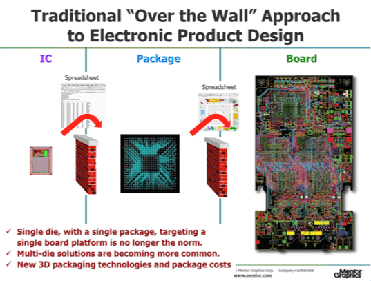
In the VS14 session on Wednesday morning John Park, methodology architect at Mentor Graphics, talked about the importance of holistic planning and showed us how Mentor solves this important need. He explained how critical it is for the success of a system design to consider the die–package–board interactions. Just like nobody in his right mind would throw an IC design “over the wall” to the layout person any more, no IC designer should try to throw a die “over the wall” to the IC packaging department. Likewise a package designer can’t throw his output “over the wall” to the PCB designers. Up-front planning, now called “Pathfinding” as well as downstream and upstream communication between design steps and also to manufacturing partners needs to replace the traditional “Over the Wall Methodology”!
 John Park also talked about how the tools in his product line can optimize PCB layout, simplify package substrate design and help reducing power dissipation, while increasing performance on the package-, board and system-level. He also shared a few ideas how to integrate die-level consideration in Mentor’s current tools and design flows.
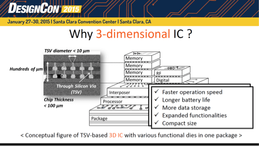
When listening to other DesignCon presenters and discussing with exhibitors on the floor, I noticed increasing interest in path finding, some call it holistic planning, as an essential method for success. Future applications will certainly demand higher frequencies, better overall performance versus power ratios and smaller form-factors from the next-generation systems. These goal can be much better and faster achieved with higher levels of integration, like using Interposer and 3D IC designs, and with the use of path finding tools and methodologies.
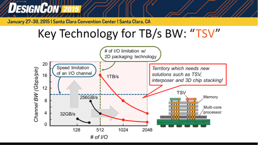
Talking about today’s high frequencies and to prepare for even higher ones, I captured some hard data at DesignCon and would like to ask system architects and designers to consider these facts when evaluating the value of reducing their systems’ form-factor. Interposer- and 3D-IC designs, can, in spite of initially higher IC component cost, save you a bundle on overall system cost and certainly improve its performance versus power ratios.
For example, Rambus demonstrated their high-speed signaling expertise in session 1-WE1 on Wednesday morning. Wendem Beyene and Jochee Kim demonstrated in a clear and compelling way how important it is to combine multiple dice in an IC package and how the ultra-wide data buses in interposer and 3D-IC designs enable cost-effective, low power AND high bandwidth designs.
Another Rambus presentation (8-WE2) on Wednesday morning clarified a question I had for a long time: “How much insertion loss do high-speed signals suffer on PCBs, using different materials?” See below a graph that answered this question … and should encourage system architects to minimize the use of large PCBs. You guessed right — I recommend instead to pack multiple dice into one IC package.
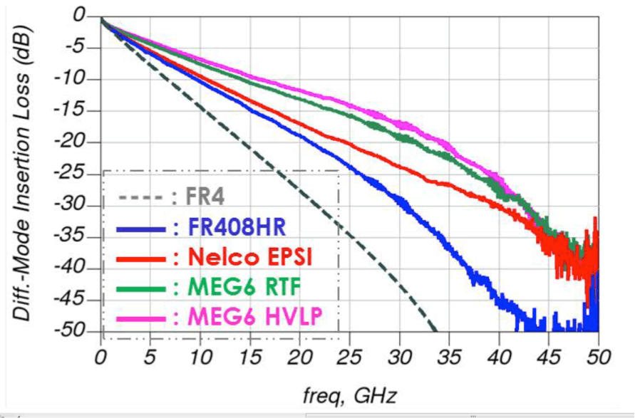 The graph shows the measured diff. insertion loss for a broad band transmission line over 12 inches of different PCB materials. Good old FR4, used since the 70s, offers low cost BUT “eats” a lot of your signal and consumes a lot of power while doing so. Other PCB materials are less hungry.

In the same presentation Yeon-Chang Hahm, Wendem Beyene, Narayan Mayandi, Don Mullen and Dave Secker (all from Rambus) also provided lots of data about insertion loss in backplanes. This area is another reason for reducing form factor, e.g. by using bare dice on an interposer or stacking dice vertically in one package.
Now you may be asking: “What is Herb doing, when he is not listening to others and learning from them?” Allow me to address this topic as well and offer you some, hopefully useful, information:
As you can tell by looking at 3D In Context, as a royal servant, I frequently blog for the Queen of 3D on 3D InCites.
I organize 3D-focused panels, presentations and entire 3D sessions at public conferences. Upon request I organize and contribute to 3D-IC focused events within interested companies. I also write and compile 3D focused documents, such as the 70-page Design Guide 2014, ready for downloading at the 3D ASIP Conference website.
In my role at Si2, contributing to the Open 3D TAB (Technical Advisory Board) is a great opportunity for me. I work with major semiconductor companies and EDA vendors. They gives me insight into large corporations’ requirements as well as their strategic and holistic thinking as it relates to 3D IC topics. Our Open 3D TAB is, as its name says, is open to everybody who wants to influence and contribute to the success of 3D technology. We define and standardize 3D-IC design flows by influencing EDA tools’ interoperability as well as data exchange formats between design steps and to the materials- and finished products supply chain.
Common data exchange formats are essential for user-friendly and high-productivity path finding tools and contribute significantly to walking the fine line between costly over-design and unreliable under-design of ICs. The Open 3D TAB just completed revision 1 of the Pathfinding specification. It is posted here, together with previously defined specifications for thermal design considerations and power distribution networks.
Our work on revision 2 is under way. If you want to inject your interposer- and 3D IC design requirements into the Open 3D TAB’s plans for 2015, please click here and answer a brief questionnaire. Please complete it and include your email address, so we can share the survey results with you. If you are interested in joining the Open 3D TAB, to help us streamline the planning and design of interposer and 3D IC designs, please contact me.
As you see in the market place, providers of mobile and consumer-applications still prefer PoP or SiP solutions. The smaller form-factor, better performance versus power ratio, cost savings on the system level and other 3D benefits can’t outweigh the currently higher component cost versus traditional solutions yet.
You can also see that less cost-sensitive applications, like networking, graphics and computing, are well on their way to deploy interposer- and 3D-IC designs. The performance versus power ratio clearly outweigh the initially higher component cost in high speed systems. For example, Nvidia managed to triple the bandwidth for their next-generation graphics solution, by combining four Hynix memory cubes with Nvidia’s GPU on an interposer.
Looking back at the very informative DesignCon 2015, is there anything I would suggest to do differently at DesignCon 2016? Yes, I would like to ask for minimizing the distances between venues. Running from the parking lot to the conference registration room at the far end, then back to the conference rooms, thereafter to the “remote” entrance for the exhibition area, and back again to the next presentation in a conference room on the other end of the convention center, was truly very good exercise. However, if people are in a hurry, they may not appreciate these long distance walks/runs. ~ Herb