


For the third consecutive January, I spent 3 days in Grenoble attending the European 3D TSV Summit. Each summit has followed a specific theme that aligned with where 3D integration was in its evolution.
Kevin Crofton, SPTS, summed it up nicely in his closing remarks this year. In 2013, we were “on the road to manufacturing”. The emphasis was on developing technology for 3D and heterogeneous stacking. The big question was, is there a supply chain? That question has since been resolved and interposer integration (formerly known as 2.5D) provided a manufacturable solution for TSV integration. In 2014, the theme was “Application Ready”, and the big question was, can TSVs be done, really? There were some significant announcements from companies like STATS ChipPAC, TSMC, Amkor, and GlobalFoundries about technology readiness. A proven supply chain had emerged for interposer integration.
This year’s topic talked about “Enabling Smarter Systems” with emphasis on the past year’s achievements in various memory-stacked products, and the anticipation of volume production of these and what it will mean for the future of 3D ICs in high volume manufacturing (HVM). Crofton said the question still remains, “when will we see heterogeneous TSV chips (memory on logic) stacked in volume production?”
During this year’s pre-conference symposium market update, as I listened to the four speakers once again discuss both technical and business motivations, enumerate remaining gaps and challenges, discuss macro and micro trends, and make predictions about when various applications will happen, it occurred to me that we have never, not in 2013 or 2014, or now, have ask the most important question of all: What does success look like for 3D integration? Because when you think about it, different stakeholders have varied agendas. Therefore success for 3D integration is a matter of perspective. This week, I started asking the question. Here are the responses I got.
- Rozalia Beica, Yole Développement, commented that while there are already products being adopted, for 3D TSVs, success means entering volume production. “We’ve overcome many challenges over the last year. This is a big achievement, even if it’s just a small step towards final success,” she said.
- “Success is when I can go into a store and buy a product to tear down and find a 3D IC inside.” said Jan Vardaman, TechSearch. Although she can’t buy one off the shelf, she said servers do count because that’s where the stacked memory will be. She also said it doesn’t necessarily need to be a consumer product.It can be industrial, or medical, but it does need to be a real product.
- Scott Jones, AlixPartners, was even more specific: “When I can go buy an iPad and it has 3D inside; when Intel and Samsung stands up here and says we have it, that’s what we see as success for this technology.”
- For Eric Beyne, imec the most important thing for success is adoption in to the market. “We need a driver for this technology,” he said. “The initial driver was a high-end product. Today we are at the point where memory cubes are a stepping stone. CMOS image sensors were important. Memory stacking is the key thing that is happening today.”
- “For Broadpak, we see two aspects of success: technology and business, said Farhang Yazdani, CEO Broadpak. “If we can achieve a low cost secure system that is easy to integrate, we call that success. On the business side, if we can make it cost effective, that will also be a success.
- Georg Kimmich, ST Microelectronics, says success for 3D is not about cost but about performance. At ST Micro, it’s already been a success for image sensors and the next step is photonics applications.
- According to, Juergen Weichart, for Oerlikon Systems success for 3D ICs means that the company’s highly ionized sputtering (HIS) PVD process will be used in high volume production, and he expects that to happen “not to long from now.” According to Weichart, HIS is capable of metallization in vias up to 20:1 aspect ratio.
- Hugo Pristauz, Besi, describes success as when there are “no more headaches” with the die bond tool. Alignment accuracy and speed they’ve got covered, he said. “The tricky part is bond control.”
- Martin Schrems, AMS, answered the question before I could ask it, using this slide of the company’s TSV roadmap to illustrate his definition of success.
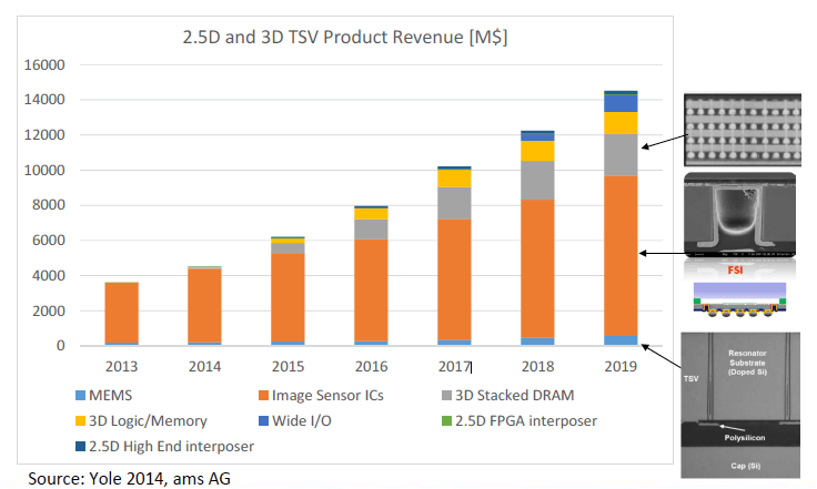
If the forecasts hold or exceed predictions for use of 3D integration and wafer-level packaging, he will consider that success. “It’s not completely unrealistic that this will happen.”

- “If we can get the first product out the door, it will be a real winner, but we don’t want to be a one-hit-wonder,” said Bryan Black, AMD. “When die stacking impacts our entire product family, that will be success for us. We think it can and are planning out how it will.”
- Offering the design perspective, Fabien Clermidy, CEA Leti, said success for 3D depends on where the products will go right now, and how different chips can be combined. “The box is open for different markets, for different ways to think about architectures, and different chips. We will pave the way for success for 3D.” he said. “All the actors are in this room to make it happen and have the chiplets available and to have good design tool technologies, and product line management, so we will see new products coming soon. The price will come down because we can obtain new chips by integrating chiplets, designing new chips and new designs.”
- Timo Henttonen said that for Microsoft, having a commercially viable product for 3D defines success. Additionally, if we can solve the test, yield and cost challenges, that is the key thing that would be a measure of success.
- While we’ve seen success with memory stacks, and via last for smaller volumes, the OSATS are stressed about getting return on investment (ROI) on the tool sets they put in, noted David Butler, SPTS. “To me, the success of 3D stacking is when the OSATS are very busy running product, and not working on three or four technology types trying to find the one that is the best, and we’re all working in the same direction.”
- For Ehrenfried Zschech, Fraunhofer IKTS, success is that they have a methodology available to validate physics-based models to get estimates for performance and reliability of 3D stacks. This allows for modeling and simulation, which reduces cost. “That’s the technical part,” he said. As a non-profit, we have to provide technical solutions to companies that enable cost reductions, so that at the end of the day, we can help companies make profits.”
- Markus Wimplinger says the ultimate success for him will be when we find a stack with memory on logic in a smartphone. “A small success will be finally stacking memories in servers this year. That is a milestone on the way to the ultimate success and what the industry is capable of,” he said. Lastly, he said a key to success on the way to the ultimate adoption of 3D technology would be to see hybrid bonding in volume production for image sensor technology. “Image sensors are the pipe cleaners for this technology because we can be a little more relaxed with device performance and shows that HVM can be done,” he said.
- Mustafa Badaraglu said that for Qualcomm, success for 3D would be achieving three criteria. First we need a low-cost agnostic solution up front. Then we need a generic assembly technology that can be leveraged across different technology nodes. Third, we need a disruptive architecture solution that takes advantage of interposer and 3D integration.
- Success in 3D for Amkor will be revenue, said Ron Huemoeller. “Success is not small business. It will be high volume,” he said. “We’ve already invested a lot and we need to see ROI.” He added that there aren’t huge hurdles to go from interposer integration to 3D. “When people are willing to design into it with faith, that will be success. It won’t take long.”
- Marco Fiorentino, HP Labs, says that for him, success in 3D will happen when we have a process that includes both the photonics and the TSV available from a foundry. “We can either design our own custom photonic circuits, or we can buy them from a supplier,” he said. “We’ve been trying to develop these things inside foundries to enrich the Si photonics ecosystem.” He issued a call to arms for collaboration on this project.
- “Saying that 3D IC is too expensive is not a good argument,” said Jürgen Wolf, Fraunhofer IZM. “You could kill every good idea with this argument. We are on the way to reducing cost for TSV. This is one step in the right direction. On the application side, I also see other technology specifications coming. We need to align the technology specs with the technology capabilities. That will bring 3D IC to success. It will happen.”
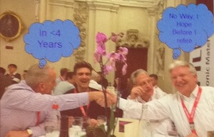 My question provoked more than annoyance at hearing me ask it over and over, it sparked some debate over dinner. Kevin Crofton predicted we would be in volume production with heterogenous stacks (logic on memory) in four years time. Thomas Leicht, Lam Research, hoped it would happen before he retires. So they decided to place a bet. The Bet: at least one memory on logic stack in four years time. The Stake: the best bottle of wine Thomas Leicht has ever had, Chateau Patreus.
So what does success in 3D integration look like for Kevin Crofton? Well, he just wants to win the bet. ~ F.v.T.


