


Ask any market researcher or business development executive at a major semiconductor manufacturing company; predicting exactly when the 3D integration market is going to take hold and fly is a tricky business, because there are so many elements to consider. During this year’s European 3D TSV Summit pre-conference market briefing, January 19, 2015, it became obvious once again that this is still a tough one to nail down. As Jim Quinn, CEO, SCINT-X, explained in his opening introduction, predictions are based on perception. He shared the anecdote about two shoe salesmen who were sent to Africa to check out the market. One came back saying there were no prospects because “no one wears shoes there.” The other came back saying there was great potential because “no one wears shoes there!”
In addition to reports by the usual suspects who have been following 3D integration for years; namely Rozalia Beica, of Yole Développement, and Jan Vardaman, TechSearch International; the summit organizing committee brought in the macro-economic perspectives of Barnett Silver, of ATREG, and Scott Jones, AlixPartners. Both presenters introduced themselves with the caveat that they knew less about advanced packaging and 3D integration than anyone else in the room. However, they offered a fresh vantage point for 3D integration that we don’t get from those who are in the trenches.
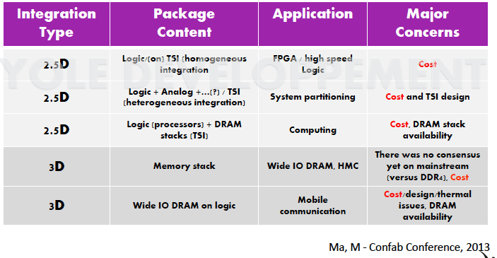
Beica reported from Yole’s latest 3D market reports, providing an up-to-date overview from development to manufacturing. “Advanced packaging is becoming more significant in this industry,” she noted, citing 28% annual growth rate, and a 19% penetration rate of wafer manufacturers relying on wafer level packaging processes such as RDL and TSVs. Beica also provided a chart that explained major concerns for product launching that could be the reason for 3D IC adoption delays. They included, predictably, cost, design, and thermal management issues. (Figure 1).
Beica also provided an update on patents, details on numerous product introduction in high performance computing, and predicted that 2015 would be the year we see 3D TSVs implemented in high volume production.
Referencing TechSearch’s recently published 3D IC gap analysis report, Jan Vardaman talked about the progress this far in high-end computing and memory stack applications, and also about where the industry needs to focus for expansion of 3D ICs. She highlighted a need for tools to assist in designing new architectures, thermal solutions for logic/memory stacks, and especially assembly/test challenges. She said currently we use the “stack and pray” method, hoping it works after we ship the stacks.
“We’re not going to get a million wafers with 3D TSV stacks until 2016, and more than half of those will be image sensors, and high performance segments of the market,” said Vardaman. Her prediction for logic and memory stack roll-out for mobile is 2018. She also noted that she’s not particularly surprised about the length of time adoption has taken. “The complexity of this has surprised people,” she said. “Any time you think you’ve solved one problem, another one comes along to solve.” She also said that because of the cost of scaling to the next silicon technology node, we have no choice but to work harder and bring 3D ICs to production. “Be patient,” she said. “It takes a long time for new technology to be adopted.”
Macro trends driving 3D adoption
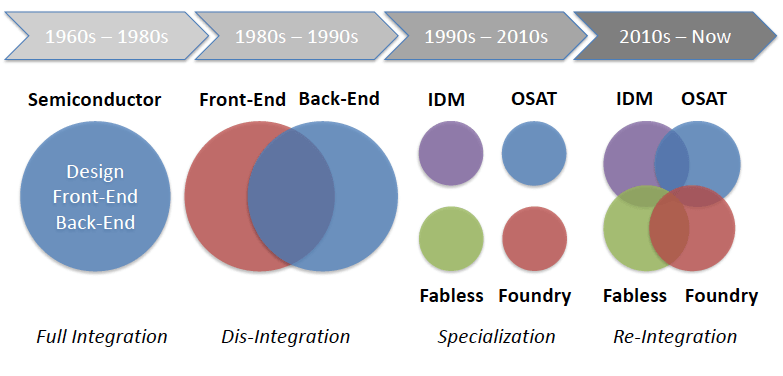
Silver talked about the future of packaging and test, focusing on the macro-trends, and whether or not there would be convergence or coexistence. “Packaging often gets over looked or under appreciated,” he said. “We think packaging is going to become a strategic differentiator for companies, with more convergence between front-and back end companies.” He also said he thinks the era of specialized companies is going to change and that we are entering a phase of reintegration of fabless, foundry, IDMS and OSATS (Figure 2).
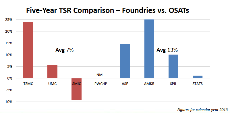
This trend, he said, is driven by 3D packaging, and the “much more attractive profit margin” it brings when compared to traditional OSAT business. This explains why foundries like TSMC are suddenly interested in getting into the assembly and test business with 3D integration. Additionally, he said, it’s not all about gross margin. Over the past 5 years, OSATS have delivered better ROI for investors than foundries (Figure 3). Thanks to 3D, the back-end business is expected to be a $51B market that is “hotly contested” by foundries, OSATS, and IDMS. Silver also predicted broad vertical integration among the fabless companies. “A theme that’s happening is companies like Google and Apple are becoming very interested in the supply chain,” he said. “Apple sees a bottleneck on the front end. I think they’ll see significance in advanced packaging.”

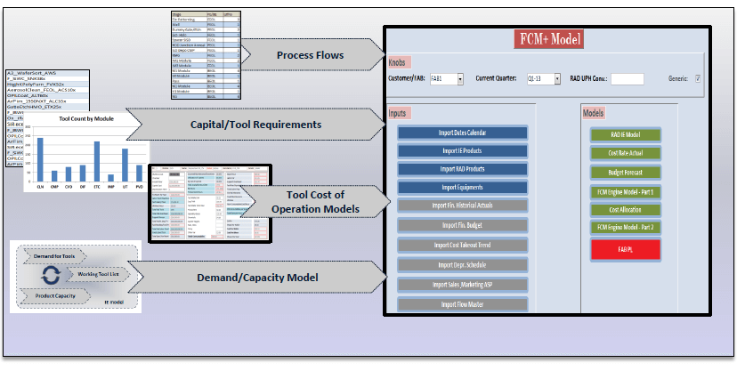
Jones took on the task of addressing cost modeling, and came up with some interesting insight when it comes to the cost of 3D and its impact on the supply chain as a whole. Rather than looking at individual costs of processes in the process flow, Jones focused on whether we are measuring the cost gap correctly. He said we should be using a full fab model vs. isolated flows (Figure 4). “These aren’t the same benefits as cost per transistor we’re used to from scaling,” he said. “How can that help us? How does 3D help in the cost take-out roadmap?
Using some examples based on different approaches and utilization times on tools in the fab, Jones demonstrated how interposer and 3D integration actually saves on total fab costs over SoC manufacturing. “A wafer gets charged ‘rent’ based on how long it spends on a tool in its journey through a fab,” explained Jones. “How much cost is it accumulating as it occupies time on the tools? What does it cost to operate the tools? What is the process complexity? How does that affect the profit and loss of the fab?” Lithography costs are increasing at faster rates due to multi-patterning. 2.5/3D can lower exposure to leading edge lithography requirements. Other advantages of 3D to consider include the ability to segregated scalable parts of a chip vs. non-scaleable. He also explained the importance of leadtime. If you miss the window, your technology can get designed out of a product. These days especially, time-to-market is especially critical. He talked about Intel’s “brown bananas”; as soon as a chip comes off the line it starts going bad. It’s important to manage lead-time and not carry risk.
In concluding his talk, Jones noted that for years, cost trends moved away from TSV interposer and 3D applications, and now it’s moving toward it. The trends are now working for us, so it’s important to understand the cost models, embrace them and understand where the crossover point happens. His parting advice: “Stack your chips high, keep your lead times short, and bananas yellow.”
Alll these different perspectives and all the analysis required to get to these conclusions confirms that predicting this market is especially tricky,. For me the key takeaway for the day was that from the macro-perspective, 3D is a worthwhile investment. Time to start selling some shoes! ~ F.v.T.


